System and method for varying wafer surface temperature via wafer-carrier temperature offset

a technology of temperature offset and wafer, which is applied in the direction of coating, chemical vapor deposition coating, metallic material coating process, etc., can solve the problems of non-uniform deposition of epitaxial growth layers on the wafer, reduced wafer yield, and reduced wafer quality, so as to reduce the effect of mass-transport edge effects

Inactive Publication Date: 2007-08-16
VEECO INSTR
View PDF31 Cites 76 Cited by
  • Summary
  • Abstract
  • Description
  • Claims
  • Application Information

AI Technical Summary

Benefits of technology

[0004] What is needed is a system and method for uniformly heating a wafer substrate that permits even co

Problems solved by technology

Disadvantageously, edge effects can result in not only non-uniform deposition of epitaxial growth layers on the wafer, but also migration of impurities into parts of the wafer, and even, in some circumstances, warping of the wafer into a “potato-chip” like shape.
This can result in reduced wafer yield, reduced wafer qual

Method used


Image

  • System and method for varying wafer surface temperature via wafer-carrier temperature offset
  • System and method for varying wafer surface temperature via wafer-carrier temperature offset
  • System and method for varying wafer surface temperature via wafer-carrier temperature offset

Examples


Embodiment Construction

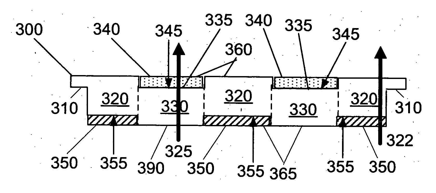
[0026] Substantial improvement in the uniformity of wafer heating has been found by adjusting the number of interfaces between materials forming the structure of a wafer carrier, such that the interfaces between the wafer carrier and a wafer (where edge effects sometimes occur) are counteracted by additional interfaces within the wafer carrier itself between a first wafer carrier material and a second wafer carrier material in those regions of the wafer carrier where wafer compartments are not present.

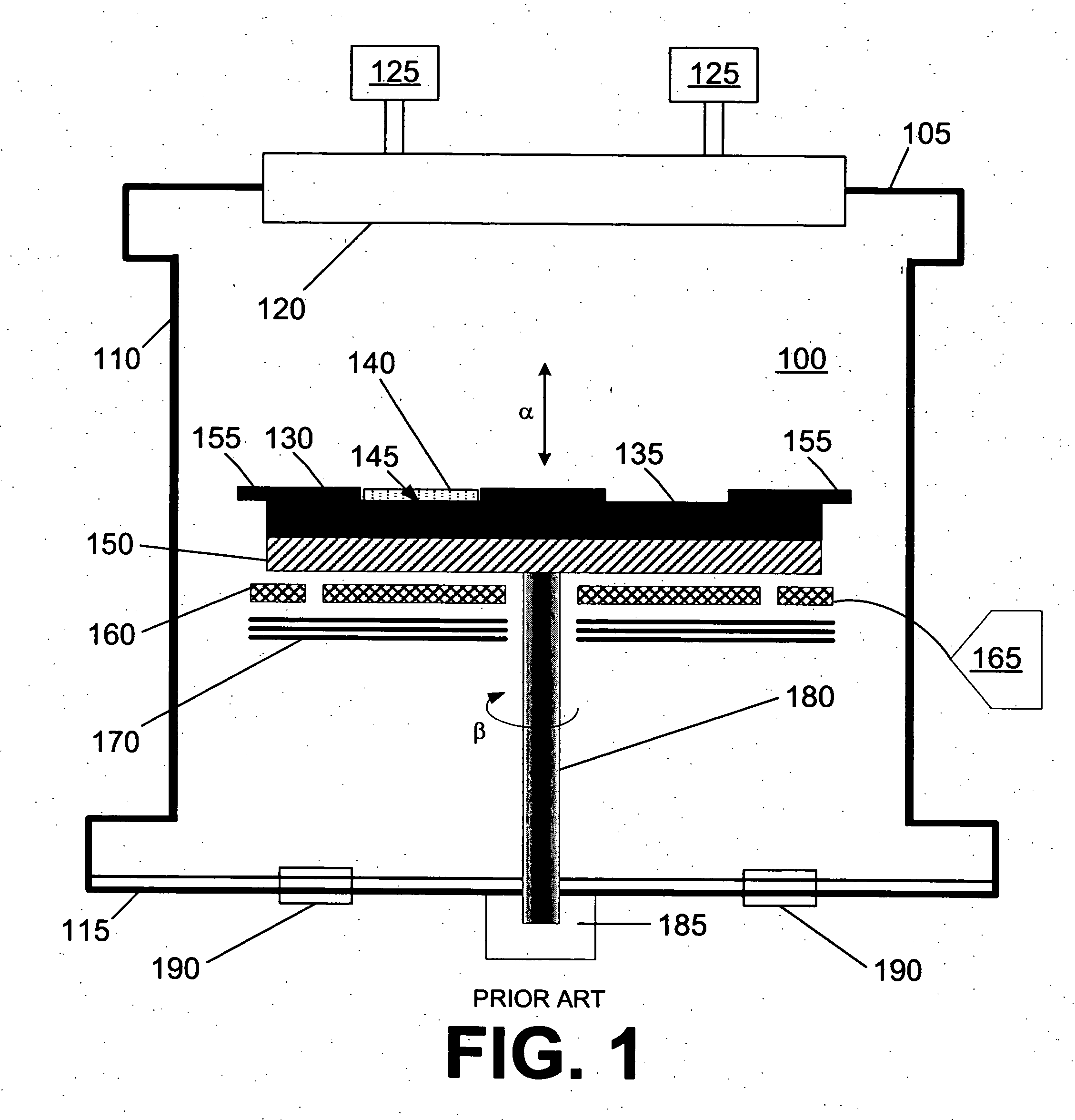
[0027]FIG. 1 shows a simplified diagrammatic cross-sectional view of a prior art chemical vapor deposition reactor. A reaction chamber 100 is defined by a chamber top 105, chamber walls 110, chamber bottom 115, and a chamber head or flange 120. The head or flange 120 is coupled to one or more sources of gasses 125 which enter the chamber 100 via the head or flange 120 to participate or assist in the reaction at or near one or more wafer substrates 140 placed in one or more wafer compa...


PUM

PropertyMeasurementUnit
Widthaaaaaaaaaa
Widthaaaaaaaaaa
Widthaaaaaaaaaa

Abstract

A system and method for evenly heating a substrate placed in a wafer carrier used in wafer treatment systems such as chemical vapor deposition reactors, wherein a first pattern of wafer compartments is provided on the top of the wafer carrier, such as one or more rings of wafer carriers, and a second pattern of inlaid material dissimilar to the wafer carrier material is inlaid on the bottom of the wafer carrier, and the second pattern of inlaid material is substantially the opposite of the first pattern of wafer compartments, such that there are at least as many material interfaces in intermediate regions without wafer compartments as there are in wafer carrying regions with wafers and wafer compartments.

Description

BACKGROUND OF THE INVENTION [0001] Uniform heating is important to many industrial applications, including chemical vapor deposition processes as applied to thin substrates such as Si or GaN based wafers. In some chemical vapor deposition systems, one or more wafer substrates are typically placed in a reactor containing a wafer carrier having one or more wafer compartments or wafer pockets. The wafer carrier and wafer substrates are then heated in the reactor, and are subjected to gasses that react near the substrate surface. This reaction results in thin epitaxial material layers developing on the wafer substrate surface, creating a desired crystalline structure thereon. The resulting processed wafers can be used in the production of end products such as, for example, integrated circuits and light emitting diodes. [0002] Compositional uniformity in layers grown on the processed wafers is important to effective wafer growth. For example, some existing substrate processing systems ha...

Claims


Application Information

Patent Timeline
IPC IPC(8): C23C16/00
CPCC23C16/4586C23C16/4581H01L21/68757H01L21/68771C30B25/12
Inventor GURARY, ALEXARMOUR, ERIC A.HOFFMAN, RICHARDCRUEL, JONATHAN
Owner VEECO INSTR
Why Eureka
Try Eureka