

Wafer processing apparatus
a processing apparatus and a technology for wafers, applied in the direction of electrical equipment, adhesives, basic electric elements, etc., can solve the problems of troublesome cleaning or maintenance of each unit, other units may constitute obstacles, and it is not easy to load tape on a predetermined uni
- Summary
- Abstract
- Description
- Claims
- Application Information
AI Technical Summary
Benefits of technology
Problems solved by technology
Method used
Image

Examples
Embodiment Construction
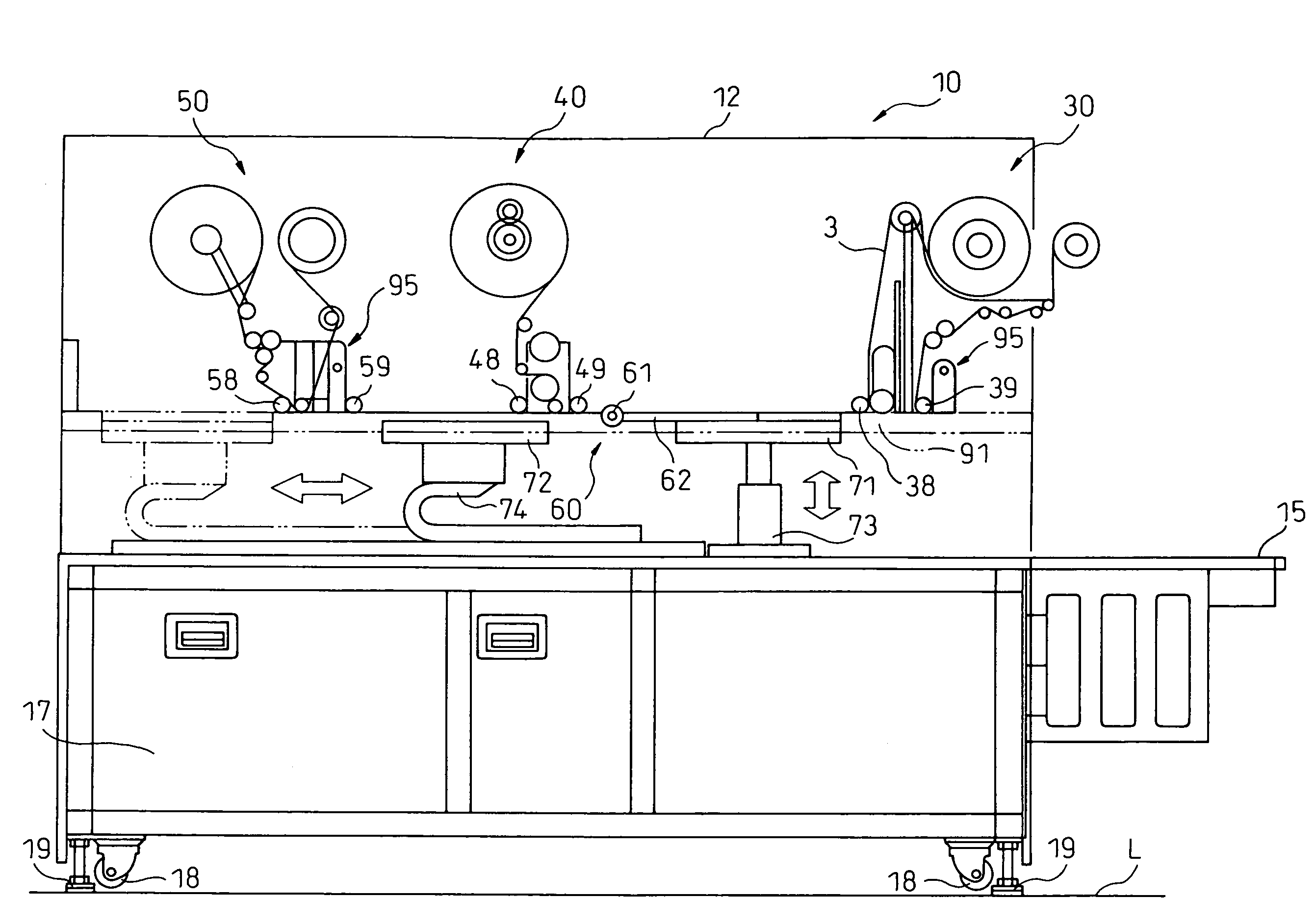
[0041]Embodiments of the invention are explained below with reference to the accompanying drawings. In these drawings, the same component members are designated by the same reference numerals, respectively. To facilitate the understanding, the scale of the drawings is changed appropriately.
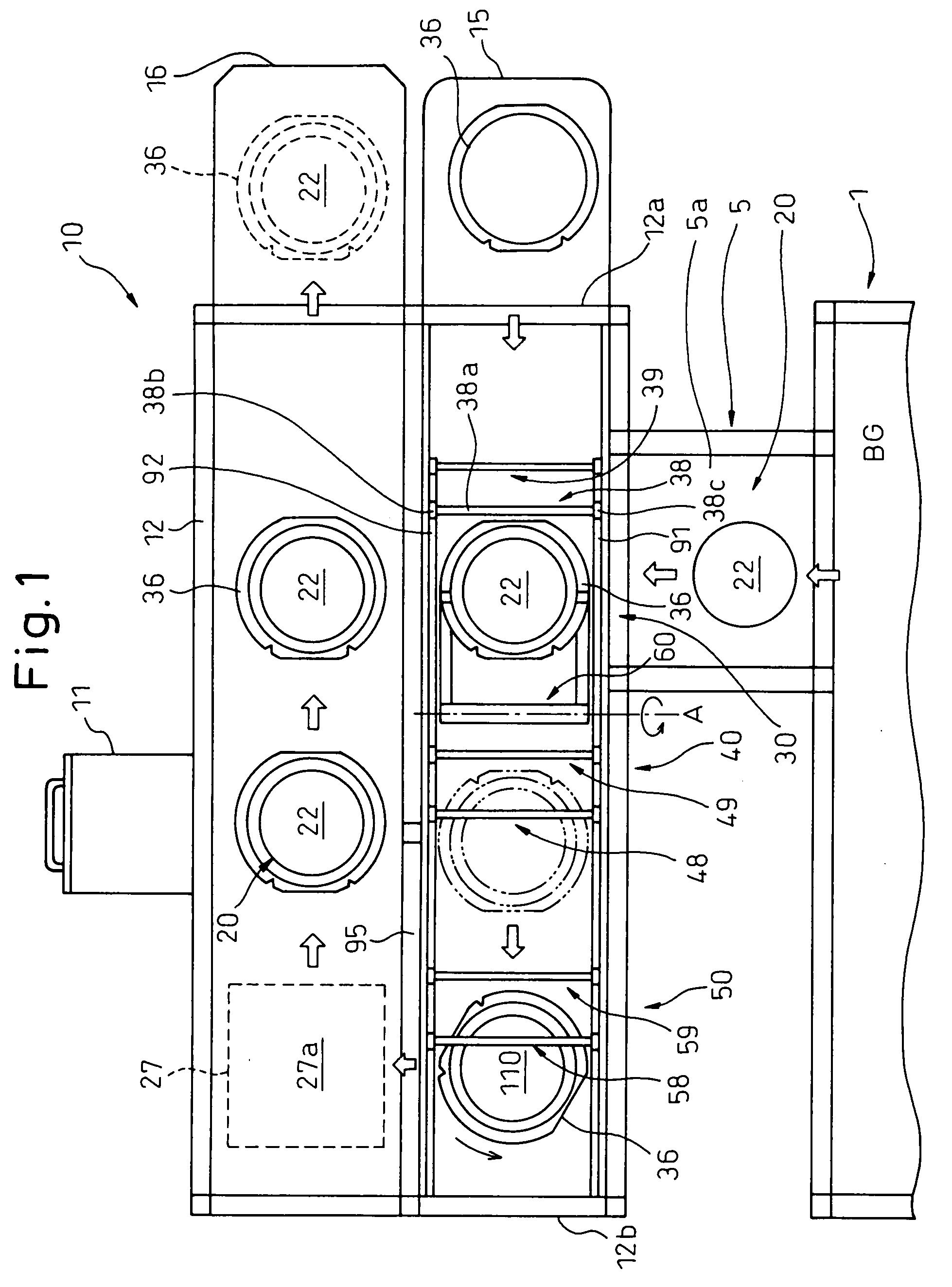
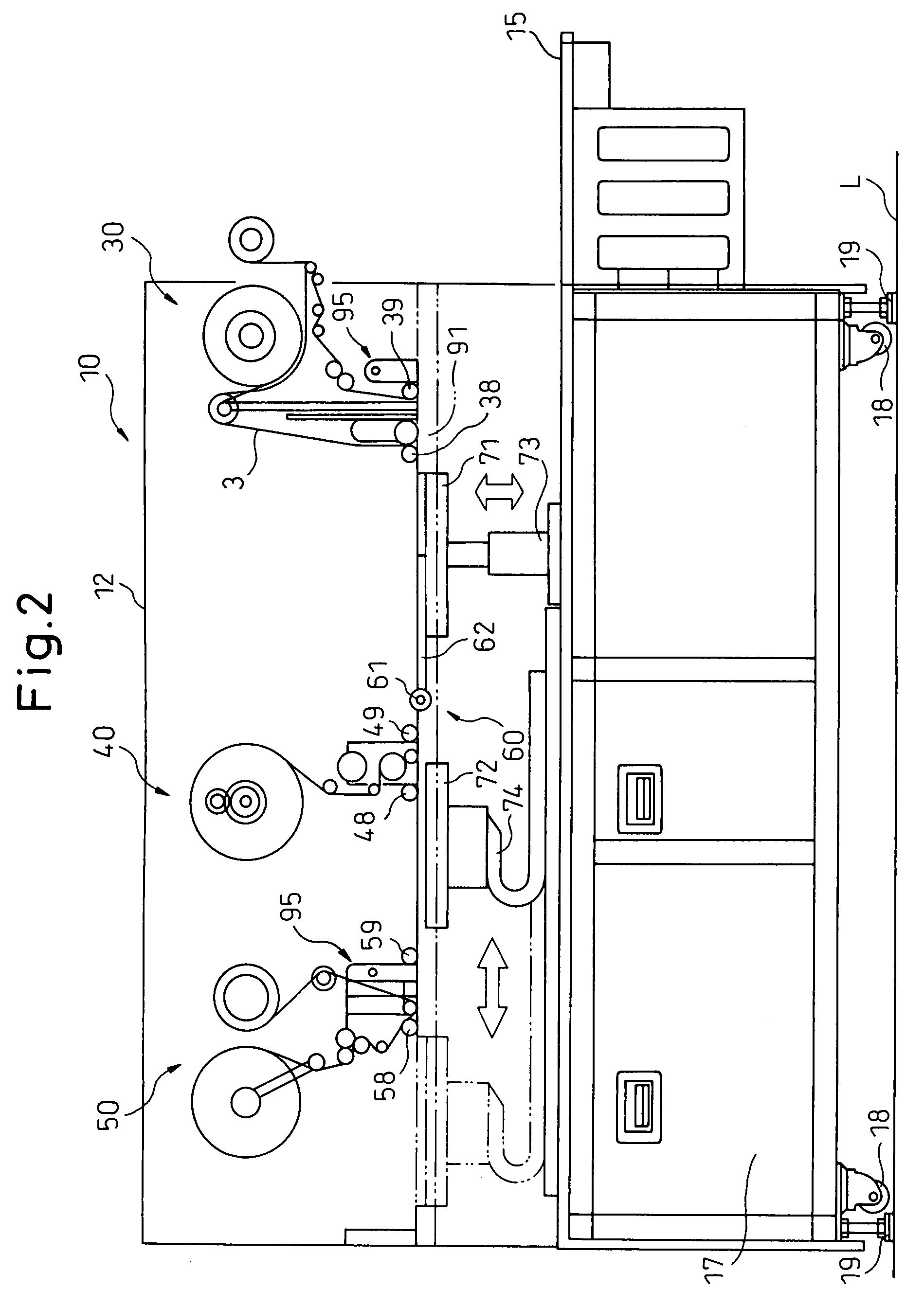
[0042]FIG. 1 is a plan view of the wafer processing apparatus according to the invention, and FIG. 2 is a side view of the wafer processing apparatus shown in FIG. 1. In FIG. 1, a wafer processing apparatus 10 is arranged adjacently to a back grinder 1. As shown in FIG. 1, the wafer processing apparatus 10 is coupled to the back grinder 1 by a first UV radiation unit (ultraviolet light radiation unit) 5.
[0043]The housing 12 of the wafer processing apparatus 10 shown in FIG. 1 includes a mount frame unit 15 in which a plurality of mount frames 36 are arranged. Also, in the housing 12, a cassette 16 for accommodating the wafers 20 integrated with the mount frames 36 is arranged removably and adjacen...
PUM
| Property | Measurement | Unit |
|---|---|---|
| thickness | aaaaa | aaaaa |
| size | aaaaa | aaaaa |
| density | aaaaa | aaaaa |
Abstract
Description
Claims
Application Information