

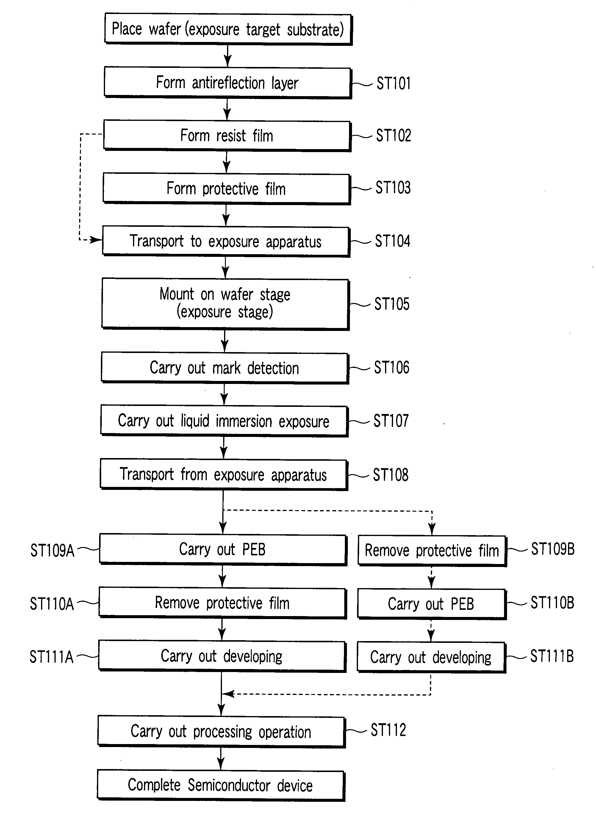
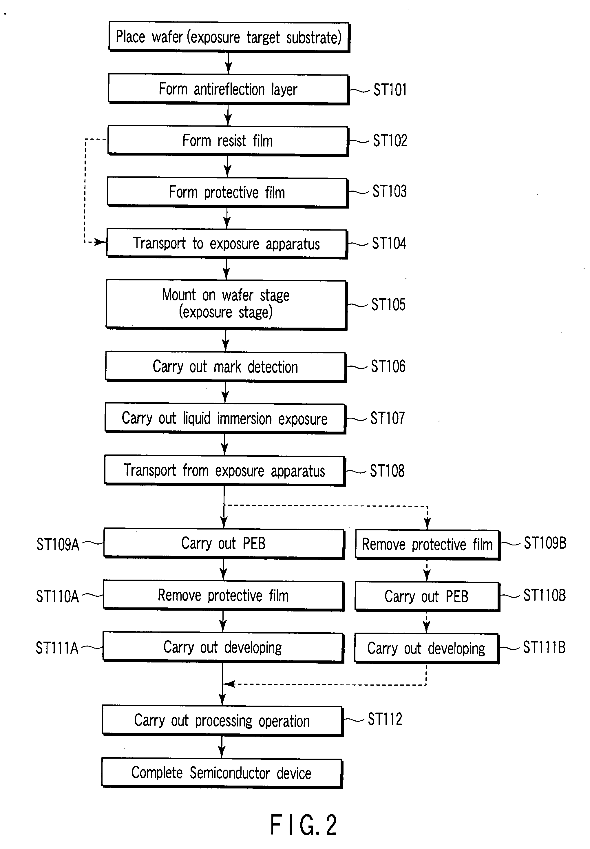
Manufacturing method of semiconductor device
a manufacturing method and semiconductor technology, applied in the field of exposure technique, can solve the problems of resist pattern formed on the resist film that cannot be moved at a high speed, liquid prone to overflow from the stage, and can not be used in liquid processing with progressive mechanical movement,
- Summary
- Abstract
- Description
- Claims
- Application Information
AI Technical Summary
Problems solved by technology
Method used
Image

Examples
first embodiment
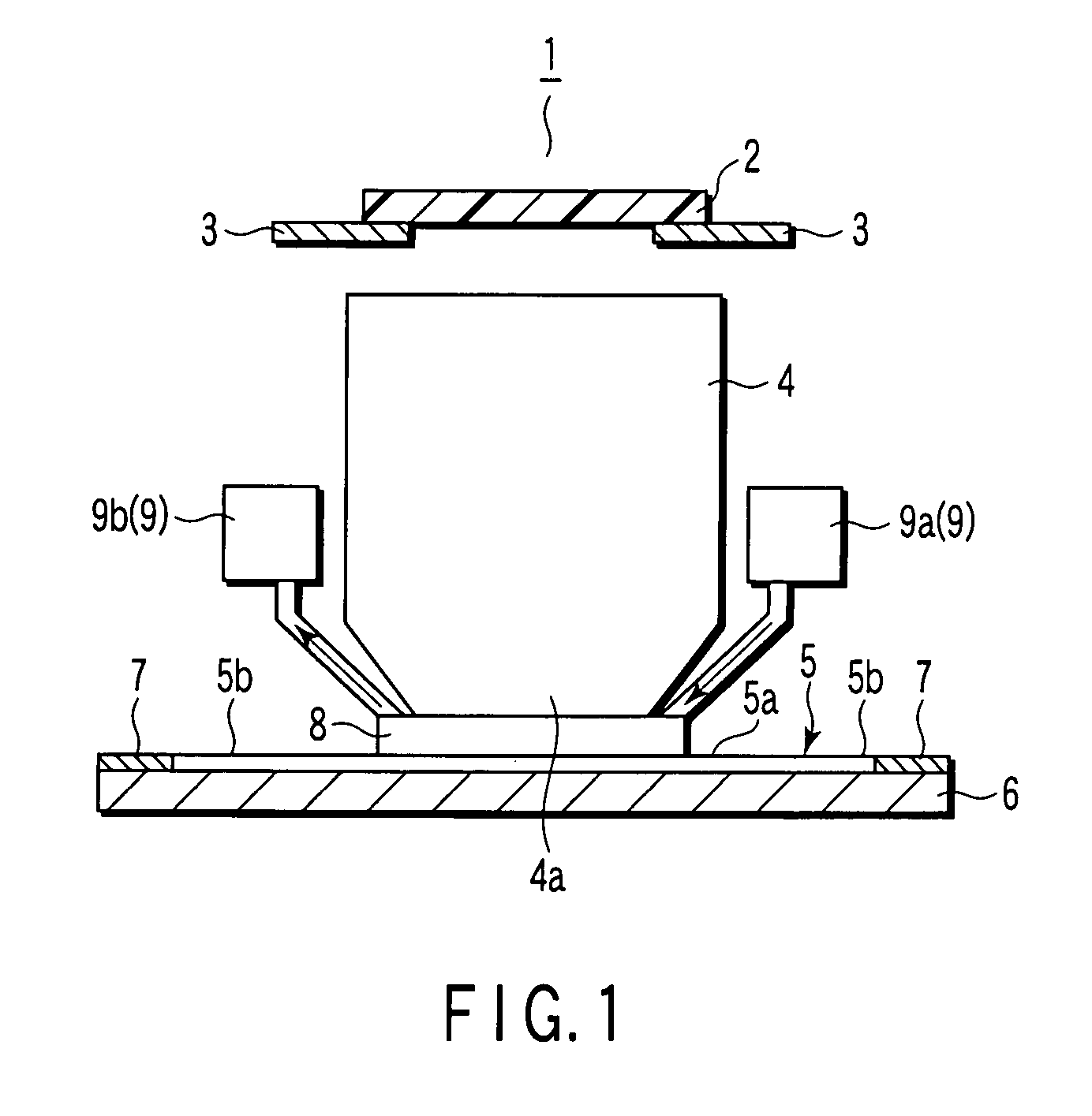
[0027] A first embodiment according to the present invention will be described with reference to FIGS. 1 to 11. The present embodiment describes a resist pattern forming method capable of restraining or reducing a risk of generating a defect on a resist pattern in a liquid immersion exposure technique for carrying out pattern exposure on a local region on a substrate passing through a liquid film. Now, a detailed description thereof will be given below.
[0028] An exposure apparatus 1 according to the present embodiment will be described with reference to FIG. 1. FIG. 1 is a view schematically depicting a general configuration of the exposure apparatus 1 for carrying out exposure processing according to the present embodiment. The exposure apparatus 1 shown in FIG. 1 is provided as a liquid immersion type exposure apparatus for carrying out so-called liquid immersion exposure, the apparatus carrying out exposure in a state in which a liquid is interposed between an exposure target su...
second embodiment
[0094] Now, a second embodiment according to the present invention will be described with reference to FIG. 12. FIG. 12 is a plan view classifying, by type of movement, a relative movement trajectory of a liquid immersion head with respect to a wafer according to the present embodiment. Like constituent elements in the first embodiment described previously are designated by like reference numerals. A detailed description thereof is omitted here.
[0095] The present embodiment describes a technique of restricting an occurrence of the residual liquid droplets in accordance with a method that is different from that of the first embodiment. Specifically, in a second liquid immersion movement process, the longest movement distance in the same direction is calculated in consideration of a movement speed of a liquid immersion region 12 (stage 6), and the liquid immersion region 12 (stage 6) is moved in a zigzag manner so that the moving distance is equal to or smaller than the acceptable lo...
third embodiment
[0100] Now, a third embodiment according to the present invention will be described with reference to FIG. 13. FIG. 13 is a plan view classifying, by type of movement, relative movement trajectory of a liquid immersion head with respect to a wafer according to a third embodiment. Like constituent elements in the first and second embodiments described previously are designated by like reference numerals. A detailed description thereof is omitted here.
[0101] The present embodiment describes a technique capable of restricting an occurrence of the remaining liquid droplets in the case where a liquid immersion region 12 passes through a rim part (outer rim part, edge part) 5b of a wafer 5 on which an exposure region 10 is not set, as well as a case in which the liquid immersion region 12 passes through the top of each exposure region 10. Specifically, when the liquid immersion region 12 passes through the edge part 5b of the wafer 5, a relative movement speed of the liquid immersion reg...
PUM
 Abstract
Description
Claims
Application Information