Resolving pattern-loading issues of SiGe stressor

a stressor and pattern-loading technology, applied in the field of sige stressor manufacturing methods, can solve the problems of pattern-loading effect drawback, affecting the performance of transistors, and non-uniform thickness of the resulting film, so as to improve the uniform improve the uniformity of the thickness of the stressor, and improve the effect of etching ra

Active Publication Date: 2007-08-16
TAIWAN SEMICON MFG CO LTD
View PDF3 Cites 43 Cited by
  • Summary
  • Abstract
  • Description
  • Claims
  • Application Information

AI Technical Summary

Benefits of technology

[0009] The preferred embodiments of the present invention provide a method of improving uniformity of stressors formed in MOS devices.
[0010] In accordance with one aspect of the present invention, the method includes forming a gate dielectric over a semiconductor substrate, forming a gate electrode on the gate dielectric, forming a spacer on respective sidewalls of the gate electrode and the gate dielectric, forming a recess in the semiconductor substrate substantially aligned with an edge of the spacer, and depositing SiGe in the recess to form a SiGe stressor. The method further includes etching the SiGe stressor to improve the thickness uniformity of the SiGe stressors.
[0011] In accordance with another aspect of the present invention, the method includes providing a semiconductor substrate including a dense region and an iso (isolated) region, forming a first gate dielectric in the dense region and a second gate dielectric in the iso region over the semiconductor substrate, forming a first gate electrode on the first gate dielectric and a second gate electrode on the second gate dielectric, forming first spacers on opposing sidewalls of the first gate electrode and the first gate dielectric and second spacers on opposing sidewalls of the second gate electrode and the second gate dielectric, forming first recesses in the semiconductor substrate substantially aligned with edges of the first spacers, forming second recesses in the semiconductor substrate substantially aligned with edges of the second spacers, depositing first SiGe stressors in the first recesses and second SiGe stressors in the second recesses wherein the second SiGe stressors have a greater growth rate than the first stressors, and etching the first and the second stressors to substantially reduce a difference in thickness between the first and the second SiGe stressors. The second SiGe stressors have a substantially greater etching rate than the first SiGe stressors.
[0012] The advantageous features of the preferred embodiments of the present invention include more uniform SiGe stressor formation, adjustable facets of SiGe stressors, and minimal extra cost.

Problems solved by technology

In accordance with a design of the transistor and one of the inherent characteristics thereof, modulating the length of a channel region underlying a gate between a source and drain of the transistor alters a resistance associated with the channel region, thereby affecting performance of the transistor.
The above-discussed method, however, suffers the drawback of pattern-loading effects, which occur due to a difference in pattern densities.
Due to a difference in growth rates of a film from one location to another, the amount of growth becomes locally dense or sparse depending on the local pattern density, and this causes non-uniformity in the thickness of the resulting film.
Large variations in effective pattern density have been shown to result in significant and undesirable film thickness variation.
Particularly, this non-uniformity makes device formation process hard to control and device performance may be adversely affected.
However, as a side effect, other epitaxy properties, such as composition, are also impacted by the changes of the pressure and gas flow rate.
Additionally, the amount of reduction of the pattern-loading effects using this method is not satisfactory.
However, additional process steps, hence higher costs, are involved.

Method used


Image

  • Resolving pattern-loading issues of SiGe stressor
  • Resolving pattern-loading issues of SiGe stressor
  • Resolving pattern-loading issues of SiGe stressor

Examples


Embodiment Construction

[0015] The making and using of the presently preferred embodiments are discussed in detail below. It should be appreciated, however, that the present invention provides many applicable inventive concepts that can be embodied in a wide variety of specific contexts. The specific embodiments discussed are merely illustrative of specific ways to make and use the invention, and do not limit the scope of the invention.

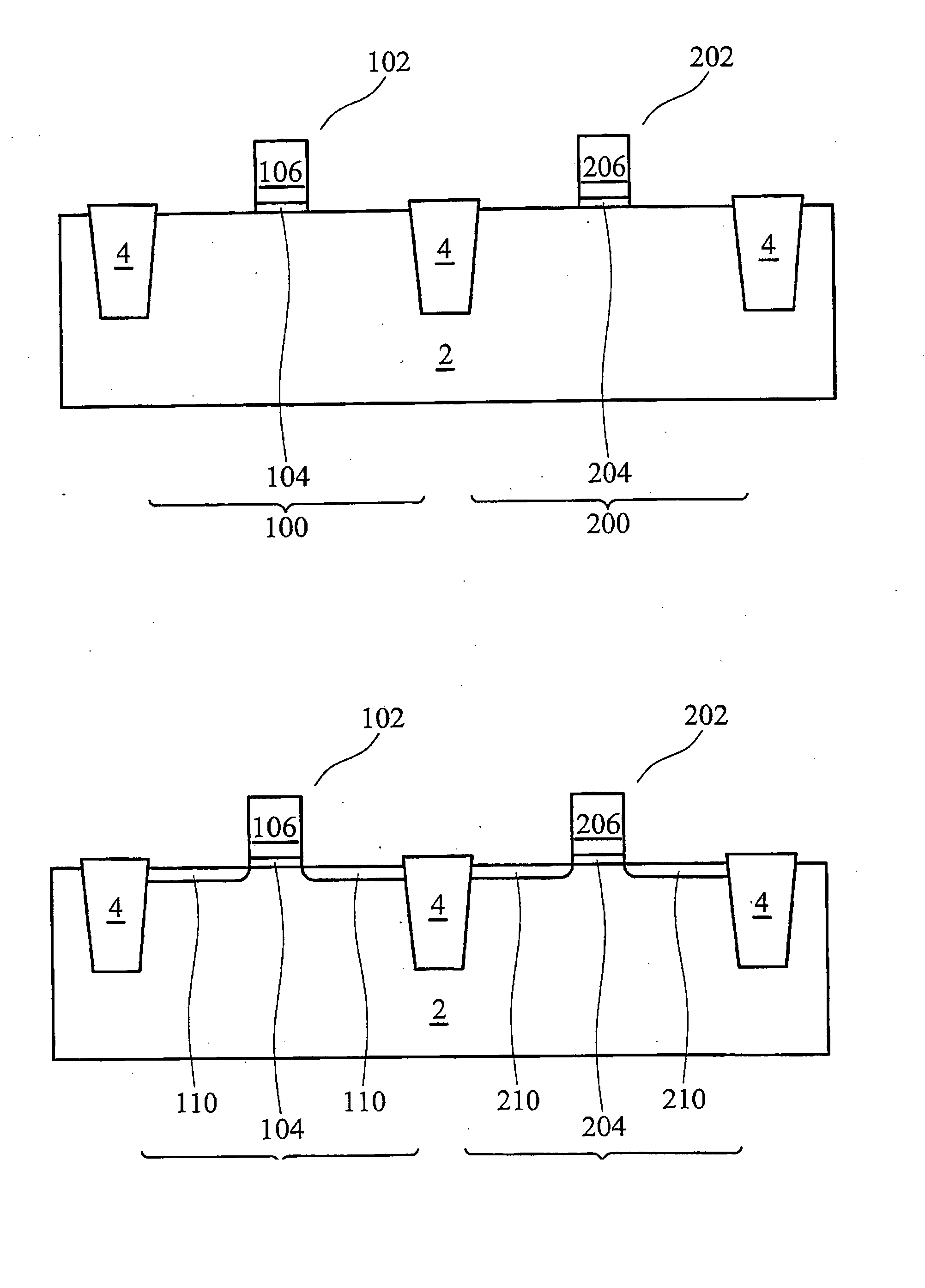
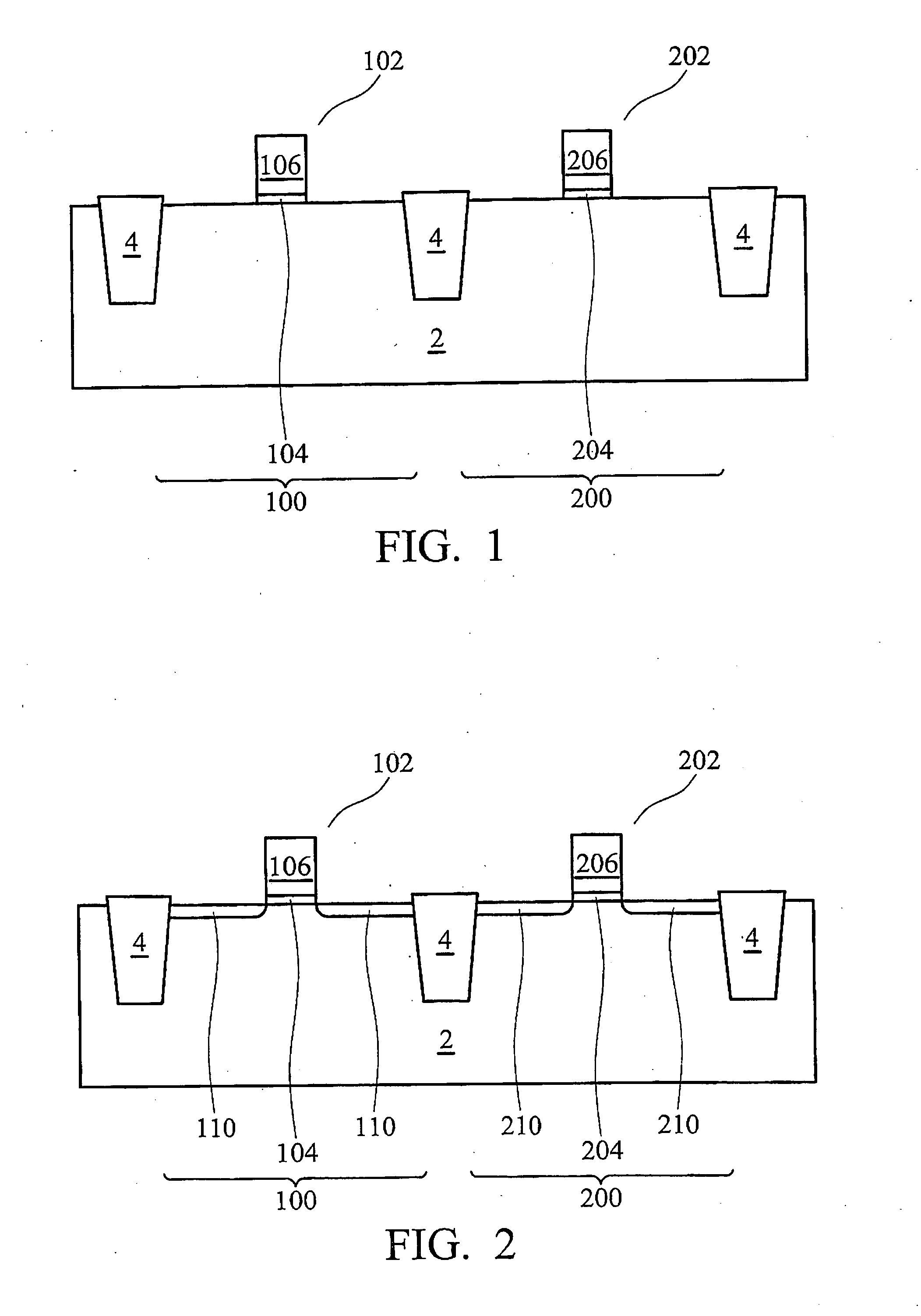
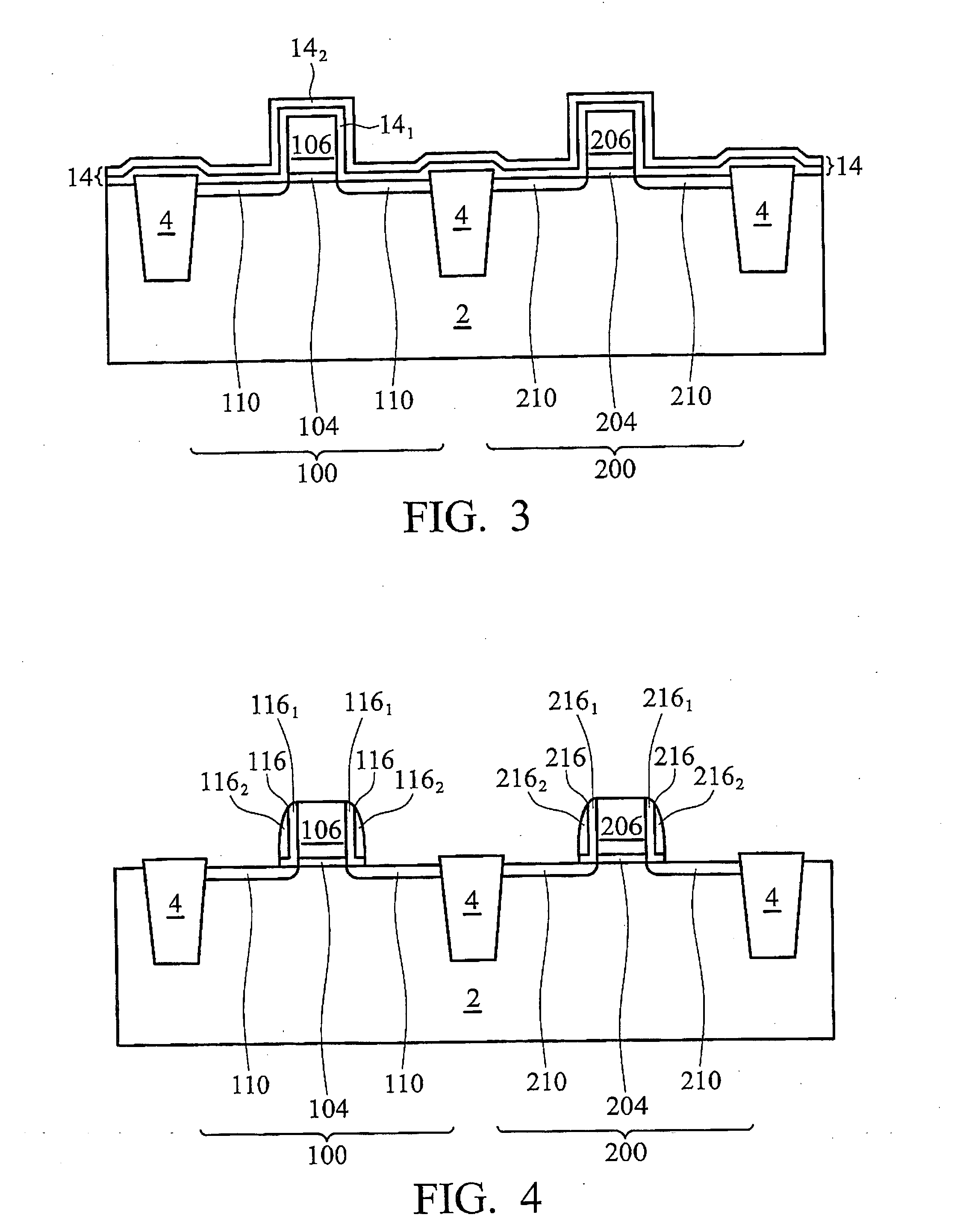
[0016] A novel method for forming PMOS devices with stressed channel regions is provided to solve pattern-loading effects (iso-dense effects) between densely patterned regions and sparsely patterned regions. The intermediate stages of manufacturing a preferred embodiment of the present invention are illustrated. Throughout the various views and illustrative embodiments of the present invention, like reference numbers are used to designate like elements.

[0017]FIG. 1 illustrates a substrate 2 including a first device region 100 and a second device region 200, wherein device ...


PUM

PropertyMeasurementUnit
depthaaaaaaaaaa
temperatureaaaaaaaaaa

Abstract

A method for improving uniformity of stressors of MOS devices is provided. The method includes forming a gate dielectric over a semiconductor substrate, forming a gate electrode on the gate dielectric, forming a spacer on respective sidewalls of the gate electrode and the gate dielectric, forming a recess in the semiconductor adjacent the spacer, and depositing SiGe in the recess to form a SiGe stressor. The method further includes etching the SiGe stressor to improve the uniformity of SiGe stressors.

Description

TECHNICAL FIELD [0001] This invention relates generally to semiconductor devices, and more particularly to a method of manufacturing PMOS devices with SiGe stressors. BACKGROUND [0002] Reduction of the size and the inherent features of semiconductor devices (e.g., a metal-oxide semiconductor field-effect transistor) has enabled continued improvement in speed, performance, density, and cost per unit function of integrated circuits over the past few decades. In accordance with a design of the transistor and one of the inherent characteristics thereof, modulating the length of a channel region underlying a gate between a source and drain of the transistor alters a resistance associated with the channel region, thereby affecting performance of the transistor. More specifically, shortening the length of the channel region reduces a source-to-drain resistance of the transistor, which, assuming other parameters are maintained relatively constant, may allow an increase in current flow betwe...

Claims


Application Information

Patent Timeline
Patent Type & Authority Applications(United States)
IPC IPC(8): H01L21/336
CPCH01L21/823807H01L21/823814H01L29/165H01L29/665H01L29/66628H01L29/66636H01L29/7848
Inventor HUANG, YU-LIENHUANG, JIMYEH, LING-YENTAO, HUN-JAN
Owner TAIWAN SEMICON MFG CO LTD
Why Eureka
Try Eureka