

Semiconductor memory and data access method
- Summary
- Abstract
- Description
- Claims
- Application Information
AI Technical Summary
Benefits of technology
Problems solved by technology
Method used
Image

Examples
Embodiment Construction
The First Preferred Embodiment
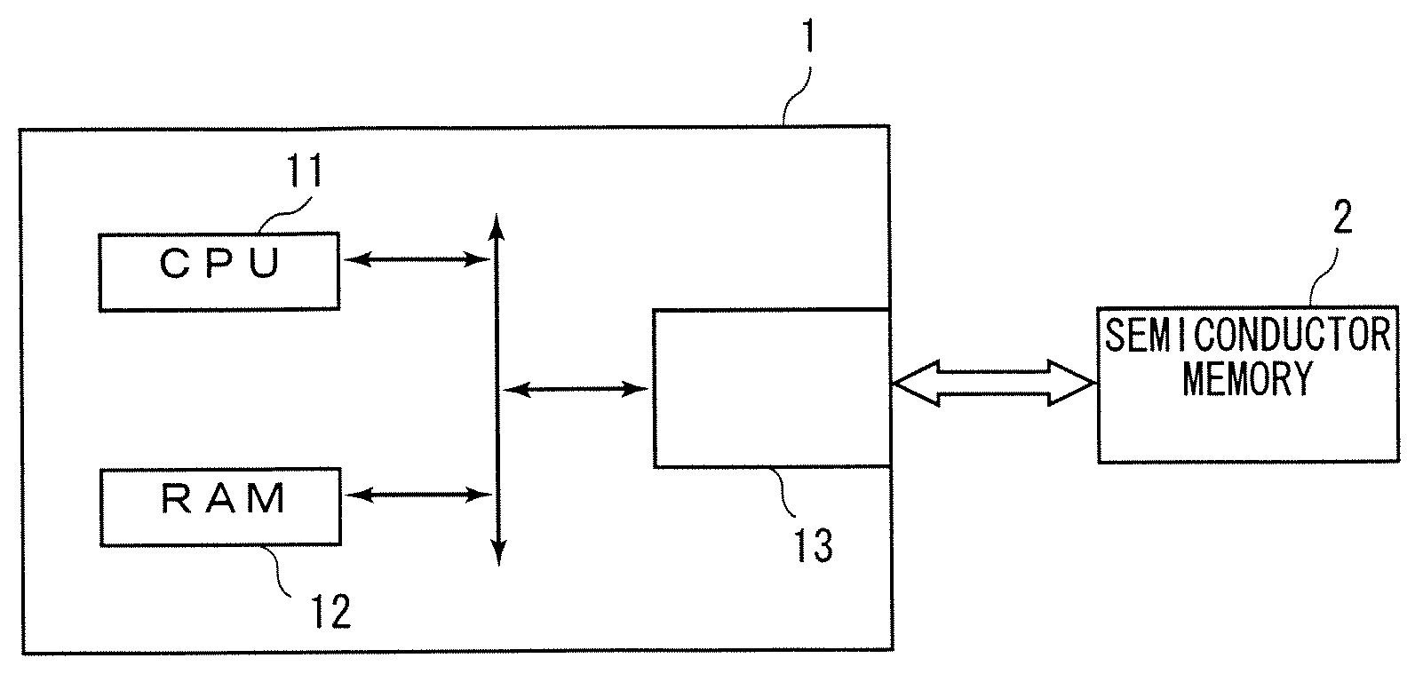
[0021]Hereinafter, the preferred embodiments of the present invention will be discussed with reference to figures. FIG. 1 is a block diagram showing an information processing apparatus 1 and a semiconductor memory 2 in accordance with the present preferred embodiment. The information processing apparatus 1 comprises a CPU 11, a RAM 12 and a memory slot 13. The information processing apparatus 1 reads out data from the semiconductor memory 2 mounted on the memory slot 13 and executes various data processings by using the CPU 11 and RAM 12. Alternatively, the information processing apparatus 1 writes data into the semiconductor memory 2.
[0022]Examples of the information processing apparatus 1 are a PDA (Personal Digital Assistance), a set-top box, a game device and the like. If the information processing apparatus 1 is a PDA or a set-top box, the semiconductor memory 2 is a memory to which an application program or content data is recorded, or if the info...
PUM
 Abstract
Description
Claims
Application Information