Photo-sensor and pixel array with backside illumination and method of forming the photo-sensor

a photo-sensor and array technology, applied in the field of pixel sensors, can solve the problems of incident angle, cmos has not been particularly suited to efficient pixel design, and the difficulty of fabricating dense cmos image sensor arrays, and achieve the effect of maximizing image sensor signal reception

Active Publication Date: 2007-08-23
SMARTSENS TECH (HK) CO LTD
View PDF9 Cites 71 Cited by
  • Summary
  • Abstract
  • Description
  • Claims
  • Application Information

AI Technical Summary

Benefits of technology

[0009] It is therefore a purpose of the invention to maximize image sensor signal reception;
[0011] It is yet another purpose of the invention to maximize the signal received by photodiodes in CMOS pixel arrays;

Problems solved by technology

Unfortunately, as pixel areas have shrunk to improve density, fabricating dense CMOS image sensor arrays has become more challenging.
CMOS has not been particularly suited to efficient pixel design because dense chip / array wiring formed above the array tends to block or diffuse light to the underlying pixels.
CMOS device structures also overlay and tend to obstruct photo-sensor diodes (photodiode).
Also, the device structures and wiring limit the incident angle at which light can be collected.
This displacement causes light to diffract.
Consequently, the image can smear due to light bleeding in from adjacent pixels.

Method used


Image

  • Photo-sensor and pixel array with backside illumination and method of forming the photo-sensor
  • Photo-sensor and pixel array with backside illumination and method of forming the photo-sensor
  • Photo-sensor and pixel array with backside illumination and method of forming the photo-sensor

Examples


Embodiment Construction

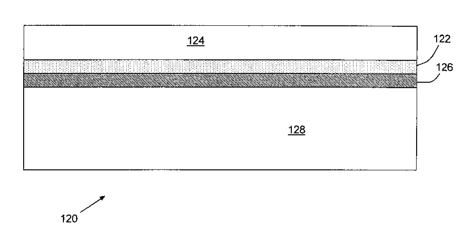
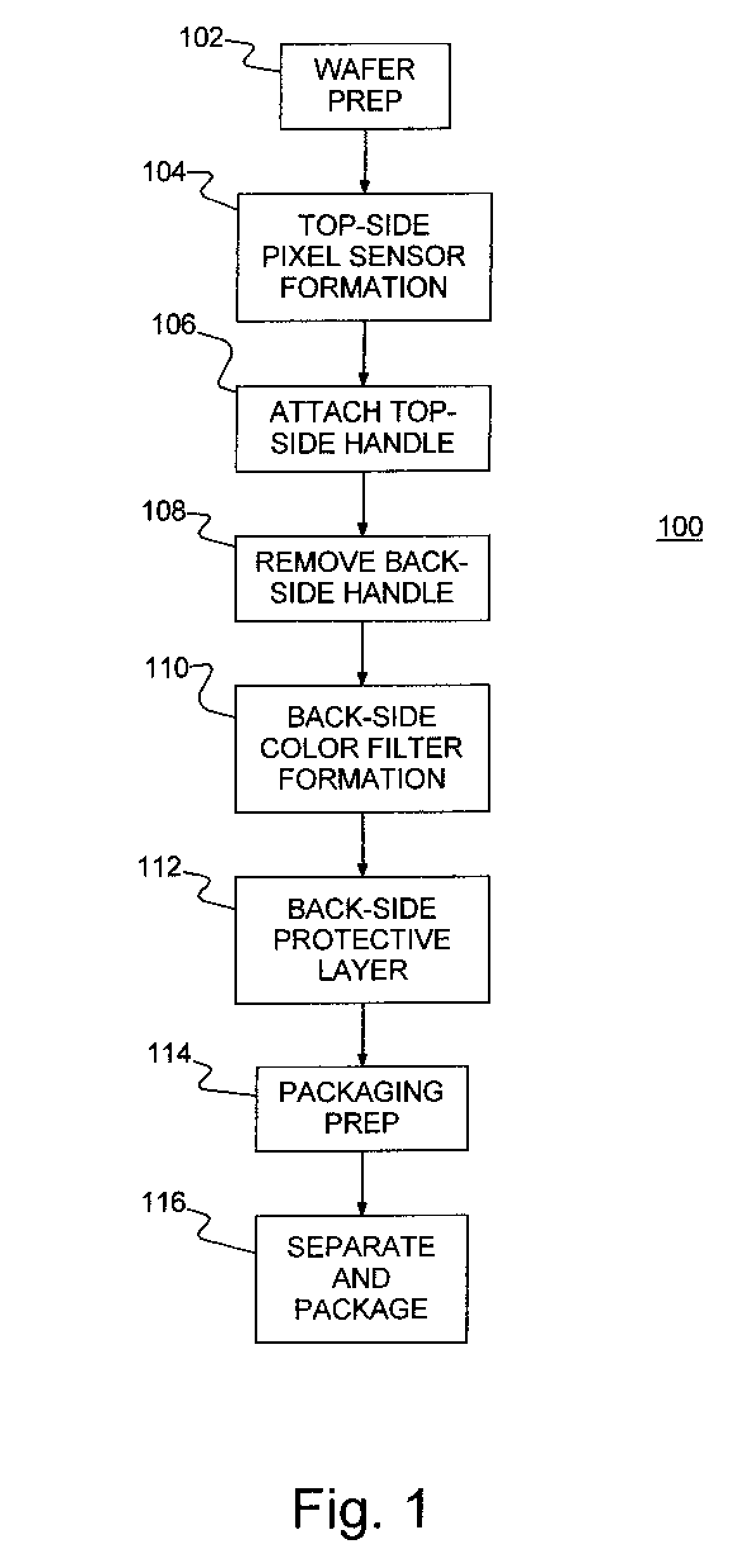
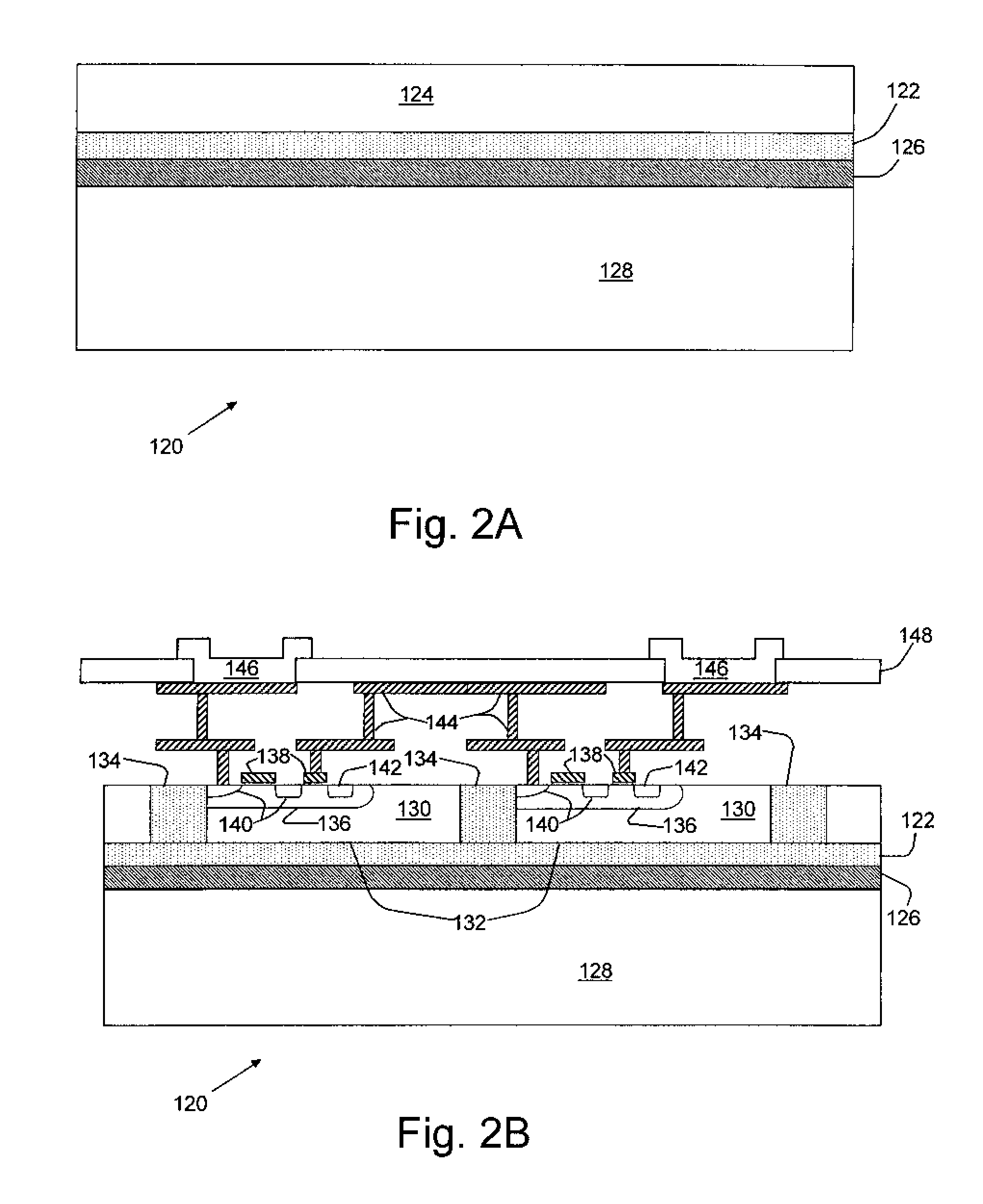
[0019] Turning now to the drawings, and more particularly, FIG. 1 shows an example 100 of forming an imaging sensor according to a preferred embodiment of the present invention. Sensor formation begins in step 102 by preparing a semiconductor wafer, e.g., by forming a dielectric layer, such as thermal oxide, on the surface of a silicon wafer. A bonding layer (e.g., nitride) is formed on the dielectric layer and a first handle wafer is bonded to the bonding layer. In step 104 image pixel sensors are formed on the exposed side of the silicon wafer, preferably, coincident with normal circuit formation. Preferably, chip circuits are formed in the insulated gate Field Effect Transistor (FET) technology commonly known as CMOS. Further, although described herein with respect to CMOS, the present invention has application to forming pixel arrays in any FET technology.

[0020] Chip circuit formation proceeds through inter-circuit wiring and, preferably to off-chip connections, i.e., in what i...


PUM


Abstract

An imaging sensor with an array of FET pixels and method of forming the imaging sensor. Each pixel is a semiconductor island, e.g., N-type silicon on a Silicon on insulator (SOI) wafer. FETs are formed in one photodiode electrode, e.g., a P-well cathode. A color filter may be attached to an opposite surface of island. A protective layer (e.g., glass or quartz) or window is fixed to the pixel array at the color filters. The image sensor may be illuminated from the backside with cell wiring above the cell. So, an optical signal passes through the protective layer is filtered by the color filters and selectively sensed by a corresponding photo-sensor.

Description

BACKGROUND OF THE INVENTION [0001] 1. Field of the Invention [0002] The present invention generally relates to pixel sensors and more particularly to CMOS image sensors. [0003] 2. Background Description [0004] Digital cameras have largely replaced film based analog cameras, at least for amateur photography. A typical digital camera image sensor is an array of picture cells (pixels), each sensing a small fragment of the light for an entire image. Generally, the higher the number of pixels, the better the resulting images (pictures) and the larger an image may be viewed before becoming pixilated. Thus, the number of pixels is a primary measure of the image resolution, and directly affects the sharpness and crispness of the resulting images. Early digital cameras included bucket brigade sensors with Charge Coupled Devices (CCDs) for pixel sensors. Integration, power, and frame rate considerations have driven the industry to convert from CCDs to image sensors that are based on more stan...

Claims


Application Information

Patent Timeline
Patent Type & Authority Applications(United States)
IPC IPC(8): H01L31/0232H01L31/00
CPCH01L27/14621H01L27/1463H01L27/1464H01L27/14689H01L27/14643
Inventor ADKISSON, JAMESGAMBINO, JEFFREYJAFFE, MARKLOISEAU, ALANRASSEL, RICHARD
Owner SMARTSENS TECH (HK) CO LTD
Why Eureka
Try Eureka