Semiconductor device and manufacturing method for the same

a technology of semiconductor devices and manufacturing methods, applied in semiconductor devices, semiconductor/solid-state device details, electrical apparatus, etc., can solve the problems of poor adhesion between different components, narrow pitch between adjacent external terminals, and peeling of the end of resin film, etc., to achieve low compatibility, high compatibility, and high performance and reliability.

Inactive Publication Date: 2007-08-23
SOCIONEXT INC
View PDF3 Cites 9 Cited by
  • Summary
  • Abstract
  • Description
  • Claims
  • Application Information

AI Technical Summary

Benefits of technology

[0012] With this method, an insulating film is first formed on a semiconductor substrate. Next, a conductive layer, which is formed of an interconnection part and a land part connecting the interconnection part to an external terminal, is formed on the insulating layer, and through holes are formed in the conductive layer at least within a part of the land part. A resin film is then formed in such a way that it passes through the through holes to thereby allow the insulating layer to contact the resin film. In this way the surface of the insulating film is in (intimate) contact with the resin film at least at a part of the land part. In contrast to a semiconductor device that adopts a structure in which the resin film which generally has low compatibility with the conductive layer is not in contact with the insulating layer for the bonding of the conductive layer and insulating layer, the semiconductor device manufactured with this method has a structure in which the resin film—a film with high compatibility with the insulating film—is allowed to contact the surface of the insulating film by passing through the conductive layer. For this reason, in this semiconductor device, the conductive layer is firmly secured to the semiconductor substrate and peeling off of the resin film end (i.e., the end of the resin film from which at least a part of the conductive layer within the land part is exposed) from the opening above the land part can be suppressed. Thus, with this method of the present invention, it is possible to manufacture a semiconductor device of high performance and reliability.

Problems solved by technology

Meanwhile, when high pin count and miniaturization of the semiconductor device are achieved as a result of increased density, it results in narrow pitch between adjacent external terminals.
However, the simpler the semiconductor device structure, the more outstanding the problem of poor adhesion between different components.
Thus, there is a problem that it is likely that the end of the resin film is peeled off due to poor adhesion between the interconnection and resin film.
The adhesion between the interconnection and resin film is susceptible to environmental conditions—the resin film is easily peeled off under heat and stress.
For example, when the semiconductor device is subjected to a high-low temperature cycle test as a reliability evaluation test, the resin film opening is degraded to cause peeling off the resin film, which sometimes leads to peeling off of the interconnection.

Method used


Image

  • Semiconductor device and manufacturing method for the same
  • Semiconductor device and manufacturing method for the same
  • Semiconductor device and manufacturing method for the same

Examples


example 1

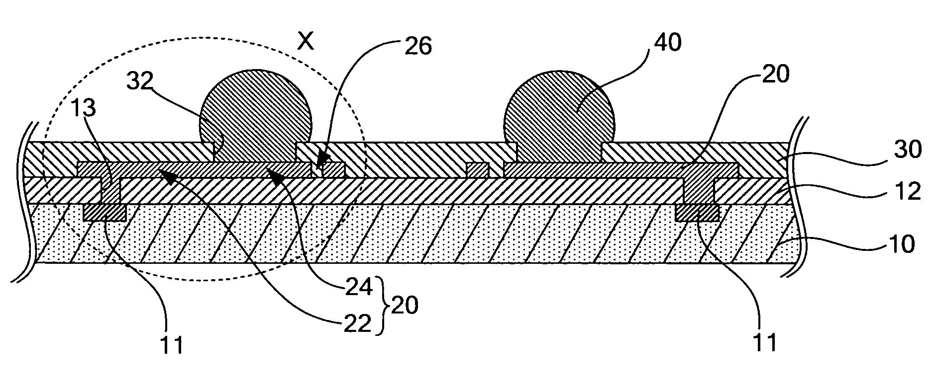
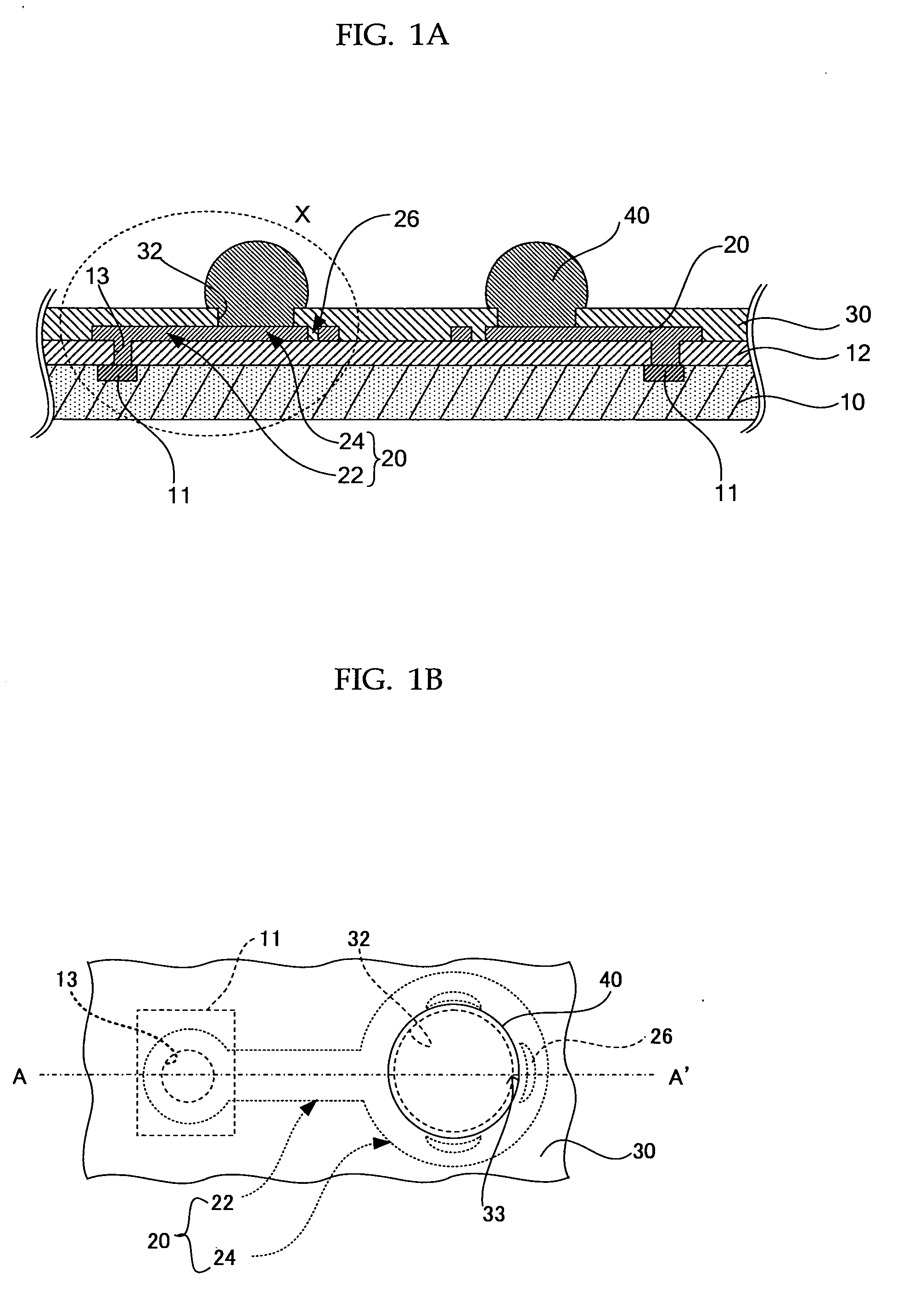
[0035] The First Example of the semiconductor device of the present invention is shown in FIGS. 1A and 1B. FIG. 1A is a cross-sectional view taken along A-A′ line of FIG. 1B, and FIG. 1B is a top view of “X” portion encircled by dotted line of FIG. 1A.

[0036] In the semiconductor device shown in FIG. 1A, an insulating film 12 made of, for example, polyimide resin, is formed on a silicon wafer 10 which has Al pads 11 and serves as the foregoing semiconductor substrate. The insulating film 12 is placed in such a way as to avoid spaces above the Al pads 11, where connection holes 13 are to be provided.

[0037] A conductive layer (or interconnection) 20 made of copper is provided on the surface of the insulating film 12, filling the connection holes 13. The Al pad 11 and conductive layer 20 are bonded together via the connection hole 13. The conductive layer 20 is formed of an interconnection part 22 and a land part 24. As shown in FIG. 1B, three through holes 26 passing through the cond...

example 2

[0062] The Second Example of the semiconductor device of the present invention is shown in FIGS. 4A and 4B. In each drawing the upper side shows the top view of the semiconductor device and the lower side shows the cross-sectional view taken along B-B′ line of the top view.

[0063] In the semiconductor device shown in FIG. 4A, there are provided four through holes 26 which are arranged substantially at equal distances from the end of the exposing opening (i.e., the end 33 of the resin film opening 32) present at least above a part of the conductive layer 20 within the land part 24, and are substantially equally spaced from one another.

[0064] Note that upon manufacturing of the semiconductor device shown in FIG. 4A, in the conductive layer formation step described above, the four through holes are formed in the conductive layer 20 in such a way that their shape, viewed from above the silicon wafer 10 horizontally divided, shows a substantially identical crescent shape and that their ...

example 3

[0065] The Third Example of the semiconductor device of the present invention is shown in FIG. 5. FIG. 5 is a top view of a land part of the semiconductor device, showing the arrangement of through holes provided above the land part.

[0066] In Example 3 there are provided eight through holes 27 passing through the conductive layer 20, as shown in FIG. 5. The eight through holes 27 have substantially identical circular shapes when viewed from above the silicon wafer 10 horizontally divided, and their size is also substantially identical. Moreover, the eight through holes 27 are arranged substantially at equal distances from the end of the exposing opening (or the end 33 of the resin film opening 32) present at least above a part of the conductive layer 20 within the land 24 part, and are also substantially equally spaced from one another.

[0067] As described above, since the eight through holes 27 are symmetrical about the center of the land part 24 in Example 3, the portions where t...


PUM


Abstract

To provide a semiconductor device with high performance and reliability, in which peeling off an interconnection layer caused due to peeling off of a resin film at a land part is suppressed and thus electrical break down is prevented, and an efficient method for manufacturing the semiconductor device. The semiconductor device includes a semiconductor substrate (e.g., a silicon wafer 10); an insulating film 12 formed on the semiconductor substrate 10; a conductive layer 20 formed on the insulating film 12, the conductive layer 20 formed of an interconnection part 22 and a land part 24 which connects the interconnection part 22 to an external terminal 40; and a resin film 30 covering the conductive layer 20, wherein the resin film 30 is in contact with the insulating film 12 at least at a part of the land part 24 by passing through the conductive layer 20.

Description

CROSS-REFERENCE TO RELATED APPLICATIONS [0001] This application is based upon and claims the benefits of the priority from the prior Japanese Patent Application No. 2006-028850 filed on Feb. 6, 2006, the entire contents of which are incorporated herein by reference. BACKGROUND OF THE INVENTION [0002] 1. Field of the Invention [0003] The present invention relates to a semiconductor device with high performance and reliability, in which peeling off an interconnection layer caused due to peeling off of a resin film at a land part is suppressed and thus electrical break down is prevented, and an efficient method for manufacturing the semiconductor device. [0004] 2. Description of the Related Art [0005] Attempts have been made in recent years to achieve downsizing and greater packaging density of semiconductor devices, with the trend moving toward for thinner, smaller electronic devices. Against this background, wafer level packaging has been proposed, which aims to achieve downsizing by...

Claims


Application Information

Patent Timeline
Patent Type & Authority Applications(United States)
IPC IPC(8): H01L23/48H01L23/52H01L29/40
CPCH01L23/3114H01L24/13H01L2224/13099H01L2924/01004H01L2924/01013H01L2924/01029H01L2924/01033H01L2924/01078H01L2924/01082H01L2924/01005H01L2924/01006H01L2924/01023H01L2924/014H01L2224/0401H01L24/05H01L2224/0231H01L2924/15787H01L2224/05556H01L2924/00H01L21/3205H01L23/12
Inventor AIBA, YOSHITAKA
Owner SOCIONEXT INC
Why Eureka
Try Eureka