Semiconductor wafer flatness correction apparatus and method

a technology of flatness correction and semiconductor wafer, which is applied in the direction of printers, instruments, ways, etc., can solve the problems of increasing product defect rates and focusing defects, and achieve the effects of preventing focus defects in exposure regions, preventing focus defects, and improving production yields

Inactive Publication Date: 2007-08-23
SAMSUNG ELECTRONICS CO LTD
View PDF2 Cites 14 Cited by
  • Summary
  • Abstract
  • Description
  • Claims
  • Application Information

AI Technical Summary

Benefits of technology

[0008]The present invention is directed to providing a wafer flatness correction apparatus and method comprising a wafer stage capable of preventing focus defects in an exposure region of a wafer. The present invention provides a wafer stage including a chuck having first and second vacuum holes, a first vacuum pump applying a vacuum suction force to the first vacuum holes and a second vacuum pump applying a vacuum suction force to the second vacuum holes. The second vacuum pump may be electrically connected to a wafer flatness correction assembly having a distance measuring unit which measures the distance to a top surface of a wafer placed on a chuck. A controller is used to compare the measured distance to a preset reference distance value, and based on the result of this comparison, controls the operation of the second vacuum pump so that the value of the measured distance and the reference value distance become equal. The controller may also control the operation of both the first and second vacuum pumps to provide suction to the wafer so that the value of the measured distance and the reference value distance become equal. This ensures that the wafer edge is sufficiently flat to prevent focus defects and improve production yields.

Problems solved by technology

Thus, the focus length becomes short causing a focusing defect and a normal circuit pattern cannot be transferred onto the edge of the wafer increases product defect rates.
When the exposure is performed onto the top surface of the wafer's edge stepped in this manner, a focusing defect may be caused as described above.

Method used


Image

  • Semiconductor wafer flatness correction apparatus and method
  • Semiconductor wafer flatness correction apparatus and method
  • Semiconductor wafer flatness correction apparatus and method

Examples


Embodiment Construction

[0018]The present invention will now be described more fully hereinafter with reference to the accompanying drawings, in which preferred embodiments of the invention are shown. This invention may, however, be embodied in many different forms and should not be construed as being limited to the embodiments set forth herein. Rather, these embodiments are provided so that this disclosure will be thorough and complete, and will fully convey the scope of the invention to those skilled in the art. In the drawings, the thicknesses of layers and regions are exaggerated for clarity. Like numbers refer to like elements throughout the specification.

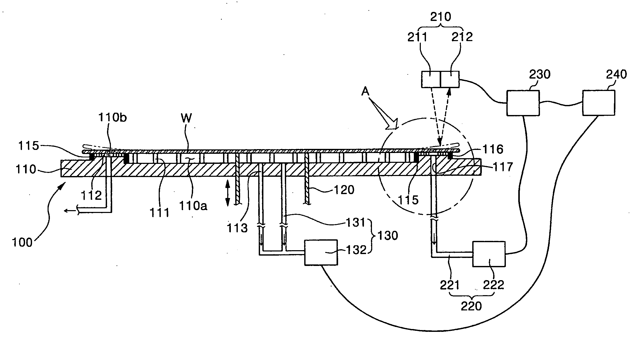
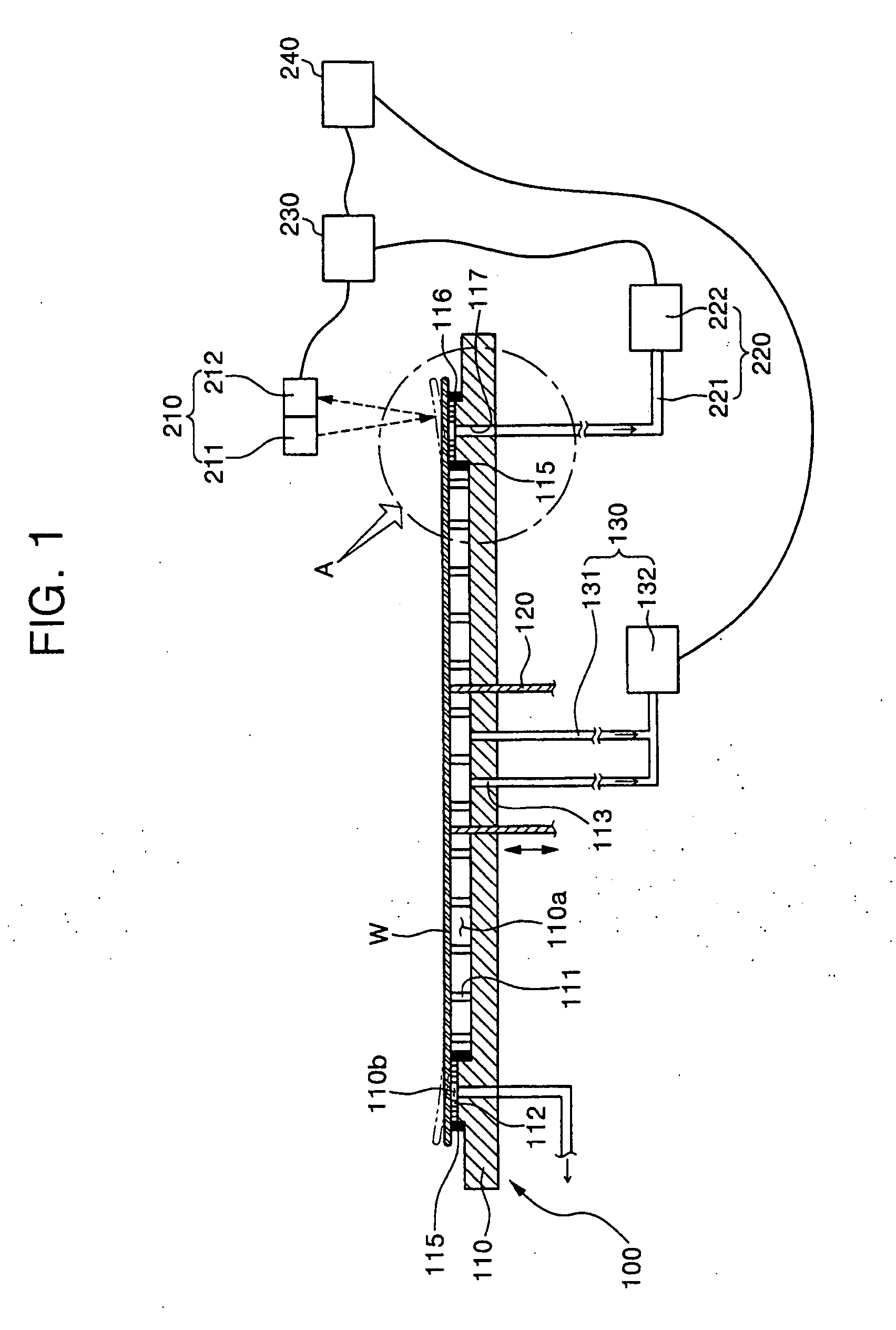
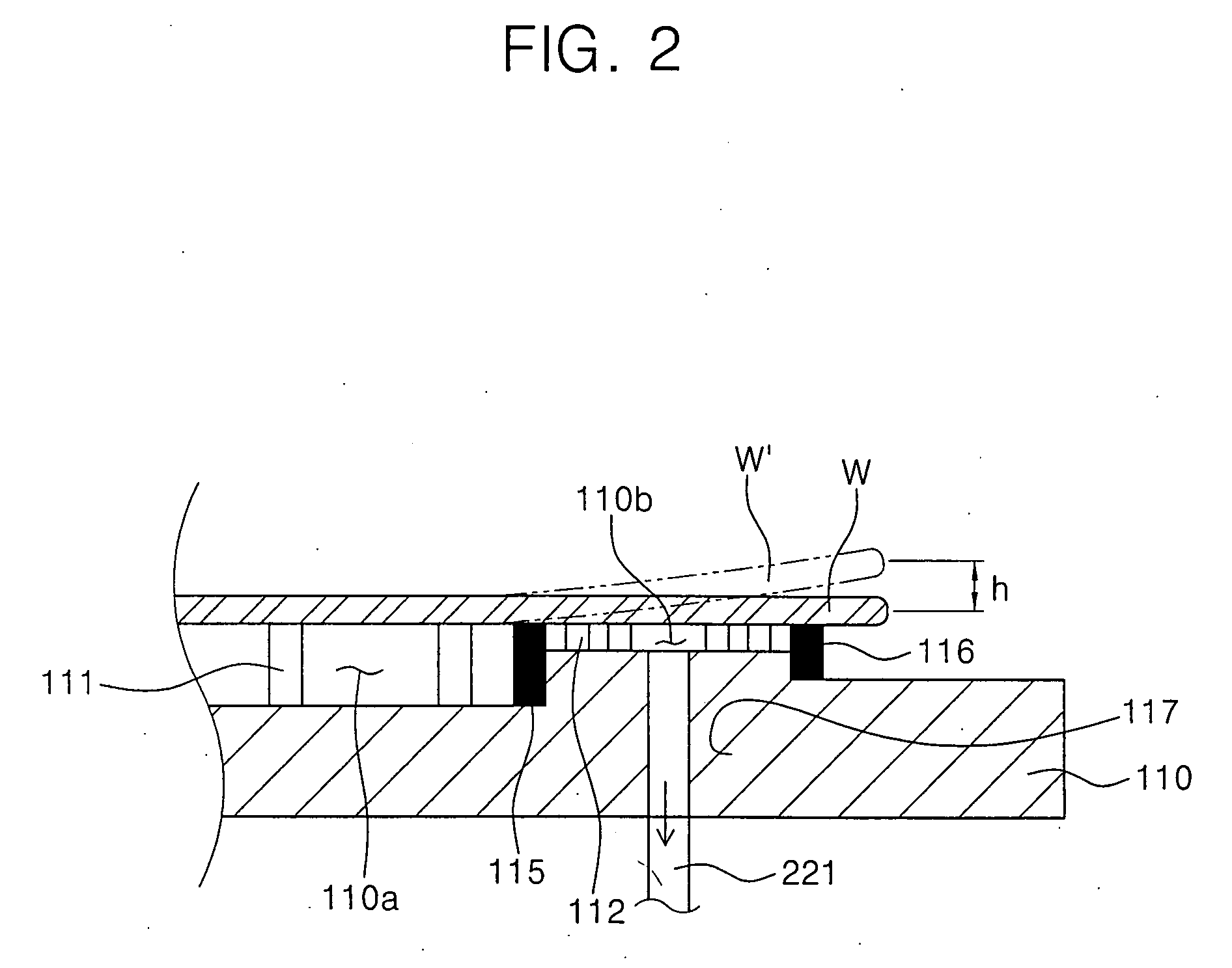
[0019]Referring to FIG. 1, a wafer stage in accordance with the present invention includes a chuck 100 through which a plurality of first vacuum holes 113 and a plurality of second vacuum holes 117 are formed. A lift pin 120 raises and lowers wafer W through a central portion of chuck 100. A first vacuum supply unit includes a first vacuum pump 132 a...


PUM


Abstract

There are provided a wafer stage, an exposure apparatus having the same, and a wafer flatness correction method using the same. The wafer stage includes a chuck having first and second vacuum holes, a first vacuum pump applying a vacuum suction force to the first vacuum holes and a second vacuum pump applying a vacuum suction force to the second vacuum holes. Further, the exposure apparatus and the wafer flatness correction method using the same are disclosed.

Description

BACKGROUND OF INVENTION[0001]1. Field of the Invention[0002]The present invention relates to a semiconductor manufacturing apparatus, and more particularly, to a wafer stage capable of correcting the flatness of a wafer placed on a chuck using a vacuum suction force and a method employing same.[0003]This application claims priority from Korean Patent Application No. 10-2006-0016465, filed Feb. 20, 2006, the disclosure of which is hereby incorporated herein by reference in its entirety as if set forth fully herein.[0004]2. Discussion of the Related Art[0005]In general, semiconductor devices are manufactured by repeatedly performing processes such as etching, diffusion, deposition, and photolithography in a selective or sequential manner. The photolithography process mainly includes an application process for applying a photoresist onto a wafer, an exposure process for disposing a reticle in which a circuit pattern is designed on the wafer on which the photoresist is applied and for r...

Claims


Application Information

Patent Timeline
Patent Type & Authority Applications(United States)
IPC IPC(8): G03B27/60
CPCG03F7/70783G03F7/707B61B1/02E01F1/00E05Y2900/404E06B11/026F16B5/02
Inventor YUN, JANG-HYUN
Owner SAMSUNG ELECTRONICS CO LTD
Why Eureka
Try Eureka