Display device

a display device and structure technology, applied in non-linear optics, instruments, optics, etc., can solve the problems of unstable wavelength dependence of absorption properties of polarizing plates, high polarization degree of polarizing plates, and difficulty in performing display with a higher contrast ratio by the method, etc., to achieve high performance display, improve the contrast ratio of display devices, and low cost

Inactive Publication Date: 2007-08-30
SEMICON ENERGY LAB CO LTD
View PDF98 Cites 51 Cited by
  • Summary
  • Abstract
  • Description
  • Claims
  • Application Information

AI Technical Summary

Benefits of technology

[0022]A structure where an extinction coefficient of an absorption axis is different from that of another absorption axis and a pair of stacks of polarizers in a parallel nicol state are provided to be deviated from a cross nicol state can prevent light leakage and further improve the contrast ratio of a display device. Further, such a high performance display device can be manufactured at low cost.

Problems solved by technology

Further, it is a problem that a polarizing plate having a high polarization degree is expensive.
A method for improving the contrast ratio by using three polarizing plates as described in Patent Document 1 can be realized by using an inexpensive polarizing plate; however, it is difficult to perform display with a higher contrast ratio by the method.
Further, a polarizing plate has unstable wavelength dependency of an absorption property, that is, an absorption property of a polarizing plate in a specific wave length region is lower than that in another wave length region.
This causes the aforementioned slight light leakage.

Method used


Image

  • Display device
  • Display device
  • Display device

Examples


embodiment mode 1

[0065]In this embodiment, a concept of a display device provided with a pair of stacks of polarizer-including layers, which uses the invention, is described.

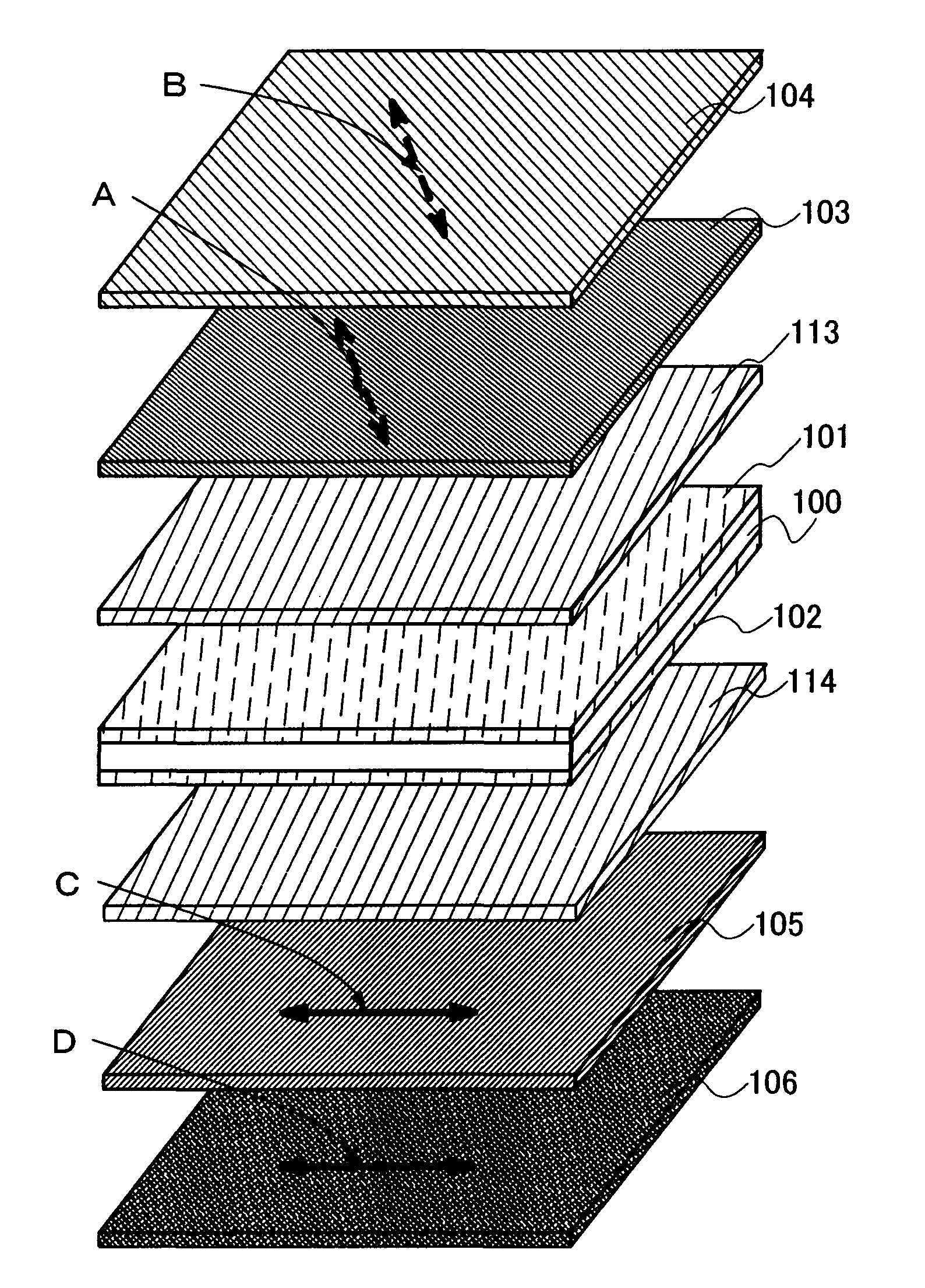
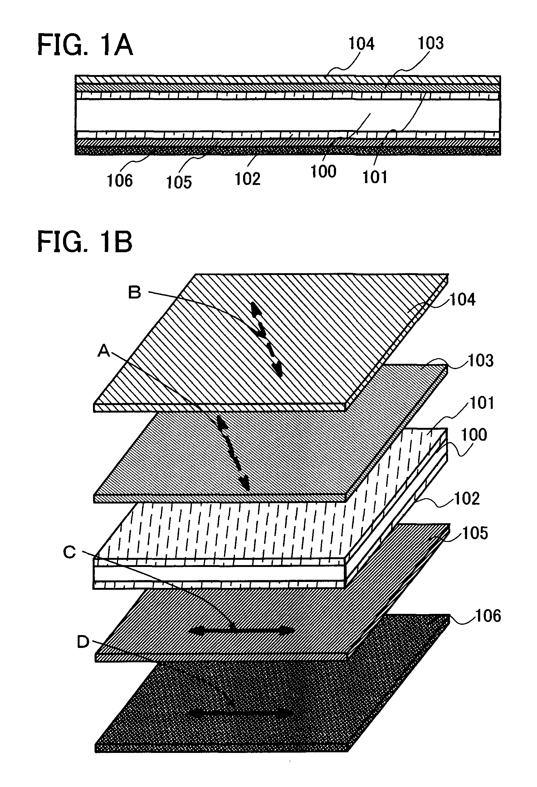
[0066]FIG. 1A shows a cross sectional view of a display device which is provided with a pair of stacks of polarizer-including layers in a parallel nicol state, in which each polarizer-including layer has a different wavelength distribution of extinction coefficient of an absorption axis, and which has a structure where one stack of polarizers and the other stack of polarizers that interpose a display element are provided so that their absorption axes are deviated from a cross nicol state, and FIG. 1B shows a perspective view of the display device. In this embodiment mode, description is made using a liquid crystal display device having a liquid crystal element as a display element, as an example.

[0067]As shown in FIG. 1A, a layer 100 including a liquid crystal element is interposed between a first substrate 101 and a second subs...

embodiment mode 2

[0081]In this embodiment mode, description is made of a concept of a display device provided with a retardation plate in addition to a pair of stacks of polarizer-including layers in which each polarizer-including layer has a different wavelength distribution of extinction coefficient of an absorption axis, which is different form the above embodiment mode.

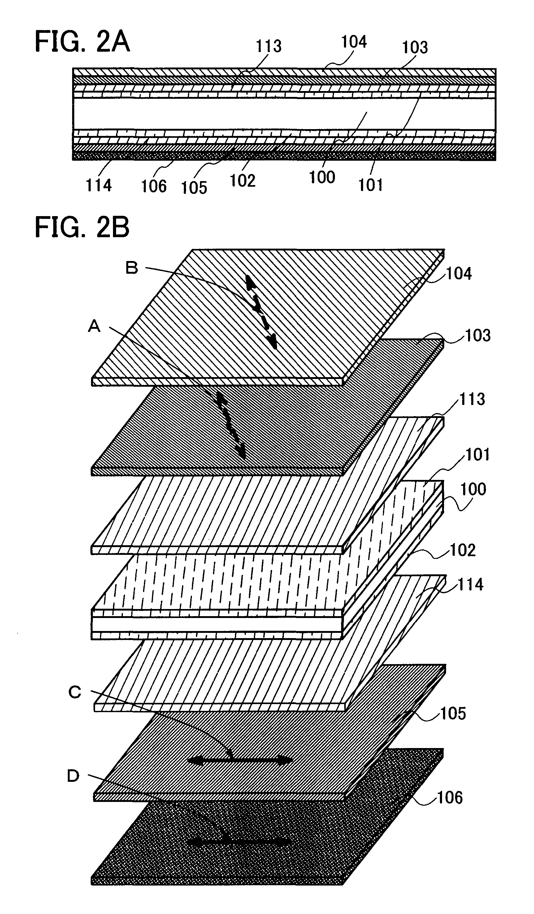
[0082]FIG. 2A shows a cross sectional view of a display device which has a structure where a pair of stacks of polarizer-including layers in a parallel nicol state, in which each polarizer-including layer has a different wavelength distribution of extinction coefficient of an absorption axis are arranged so that absorption axes of one stack of polarizers and the other stack of polarizers which interpose the display element are deviated form a cross nicol state, and which is provided with a retardation plate between one stack of polarizer-including layers and a substrate, and the other stack of polarizer-including layers and the su...

embodiment mode 3

[0098]In this embodiment mode, description is made of a structure of stacked polarizers each having a different wavelength distribution of extinction coefficient of an absorption axis, which can be used in the invention, with reference to FIGS. 13A to 13C.

[0099]In the invention, a polarizer-including layer only needs to include at least a polarizer having a specific absorption axis, and it may have a single-layer structure or a structure where a protective film is provided so as to interpose a polarizer. FIGS. 13A to 13C show examples of a stacked-layer structure of polarizer-including layers in the invention. FIG. 13A shows a stack of polarizer-including layers, which includes a polarizer-including layer formed of a protective layer 50a, a first polarizer 51, and a protective layer 50b and a polarizer-including layer formed of a protective layer 50c, a second polarizer 52, and a protective layer 50d. Thus, in the invention, a stack of polarizers also corresponds to polarizers not s...


PUM

PropertyMeasurementUnit
sizeaaaaaaaaaa
sizeaaaaaaaaaa
thicknessaaaaaaaaaa

Abstract

An object of the invention is to provide a display device having a high contrast ratio. Another object of the invention is to manufacture such a high-performance display device at low cost. In a display device having a display element between a pair of light-transmissive substrates, polarizer-including layers, which have different wavelength distributions of extinction coefficients, are stacked so that absorption axes are in a parallel nicol state, over each light-transmissive substrate. Absorption axes of one of a pair of stacks of polarizers and the other together which interpose the display element are deviated from a cross nicol state. A retardation plate may be provided between the stack of polarizing plates and the substrate.

Description

BACKGROUND OF THE INVENTION[0001]1. Field of the Invention[0002]The present invention relates to a structure of a display device including a liquid crystal element.[0003]2. Description of the Related Art[0004]A so-called flat panel display, which is a display device that is very thin and lightweight as compared to the conventional cathode-ray tube display device, has been developed. A liquid crystal display device having a liquid crystal element as a display element, a light emitting device having a self-light emitting element, an FED (field emission display) using an electron beam, and the like compete in the market of flat panel displays. Therefore, lower power consumption and higher contrast ratio are demanded in order to increase the added value and to differentiate from other products.[0005]In general, a liquid crystal display device is provided with one polarizing plate over each of substrates to keep the contrast ratio. The higher the contrast ratio is, the more clearly black...

Claims


Application Information

Patent Timeline
Patent Type & Authority Applications(United States)
IPC IPC(8): G02F1/1335
CPCG02F2001/133531G02F1/133533G02F1/133531G02F1/1335
Inventor EGI, YUJIISHITANI, TETSUJINISHI, TAKESHI
Owner SEMICON ENERGY LAB CO LTD
Why Eureka
Try Eureka