

Vertical cavity surface emitting laser
a laser and vertical cavity technology, applied in the direction of lasers, lasers, semiconductor lasers, etc., can solve the problem that the photonic crystal reflector reflection band can be easily collapsed at an order of tens of several nanometers, and achieve the effect of easy collaps
- Summary
- Abstract
- Description
- Claims
- Application Information
AI Technical Summary
Benefits of technology
Problems solved by technology
Method used
Image

Examples
example 1
[0142]The vertical cavity surface emitting laser prepared in Example 1 according to the present invention will be described below.
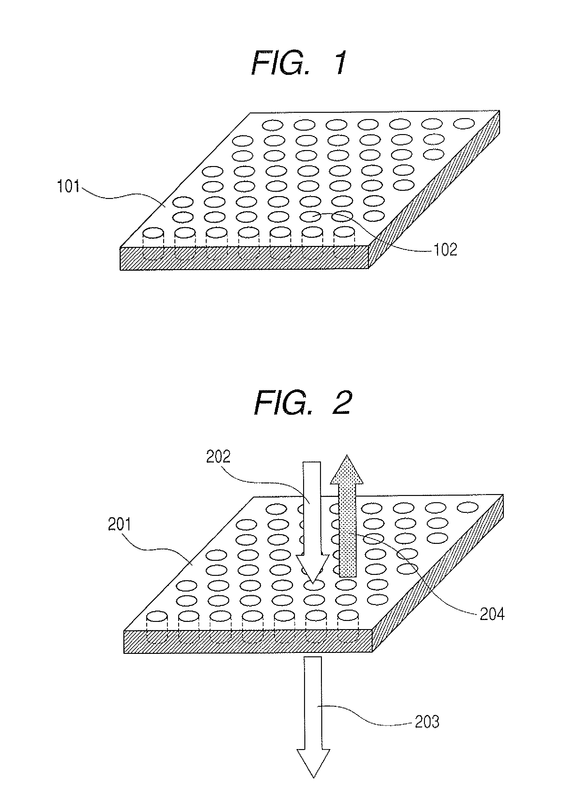
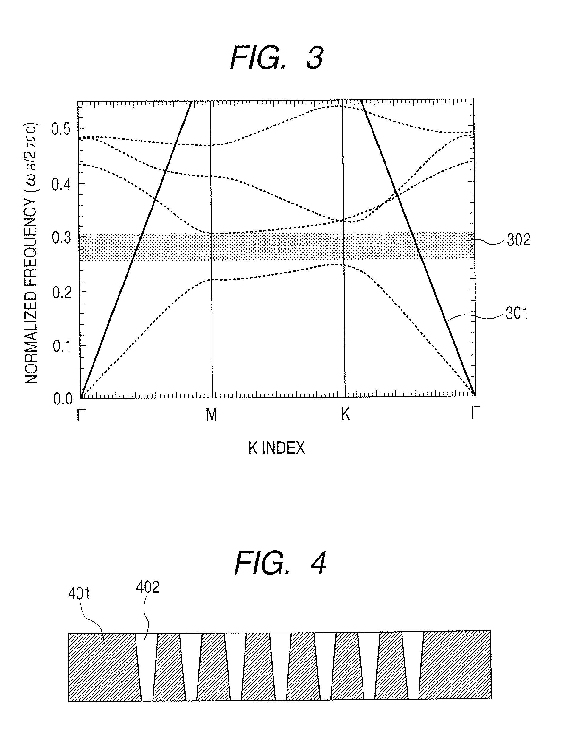
[0143]FIGS. 8A and 8B are schematic views of the vertical cavity surface emitting laser of this example, illustrating the configuration thereof. FIG. 8A is a schematic cross sectional view taken along a direction perpendicular to the substrate of the vertical cavity surface emitting laser of this example. FIG. 8B is a schematic plan view as viewed in the direction perpendicular to the surface of the cavity reflector of this example.
[0144]Referring to FIG. 8A, there are illustrated a substrate 801, a lower photonic crystal light-confining layer 802, a lower cavity reflector layer 803, lower cavity reflector photonic crystal holes 804, a lower clad layer 805, an active layer 806 and a current-confining layer 807.
[0145]FIG. 8A also illustrates an upper clad layer 808, an upper cavity reflector layer 809, upper cavity reflector photonic crystal holes 810, an ...
example 2
[0207]The vertical cavity surface emitting laser prepared in Example 2 according to the present invention will be described below.
[0208]FIG. 10 is a schematic cross sectional view of the vertical cavity surface emitting laser of Example 2 taken along a direction perpendicular to the substrate.
[0209]Referring to FIG. 10, there are illustrated a substrate 1001, a lower photonic crystal light-confining layer 1002, a lower cavity reflector layer 1003, lower cavity reflector photonic crystal holes 1004, a lower clad layer 1005, an active layer 1006 and a current-confining layer 1007.
[0210]FIG. 10 also illustrates an upper clad layer 1008, an upper cavity reflector layer 1009, upper cavity photonic crystal holes 1010, an n-electrode 1011 and a p-electrode 1012.
[0211]In this example, the substrate is a 525 μm-thick GaAs substrate and the lower photonic crystal light-confining layer is made of n-Al0.8Ga0.2As and has a thickness of 500 nm, while the lower clad layer is made of n-(Al0.5Ga0.5)...
example 3
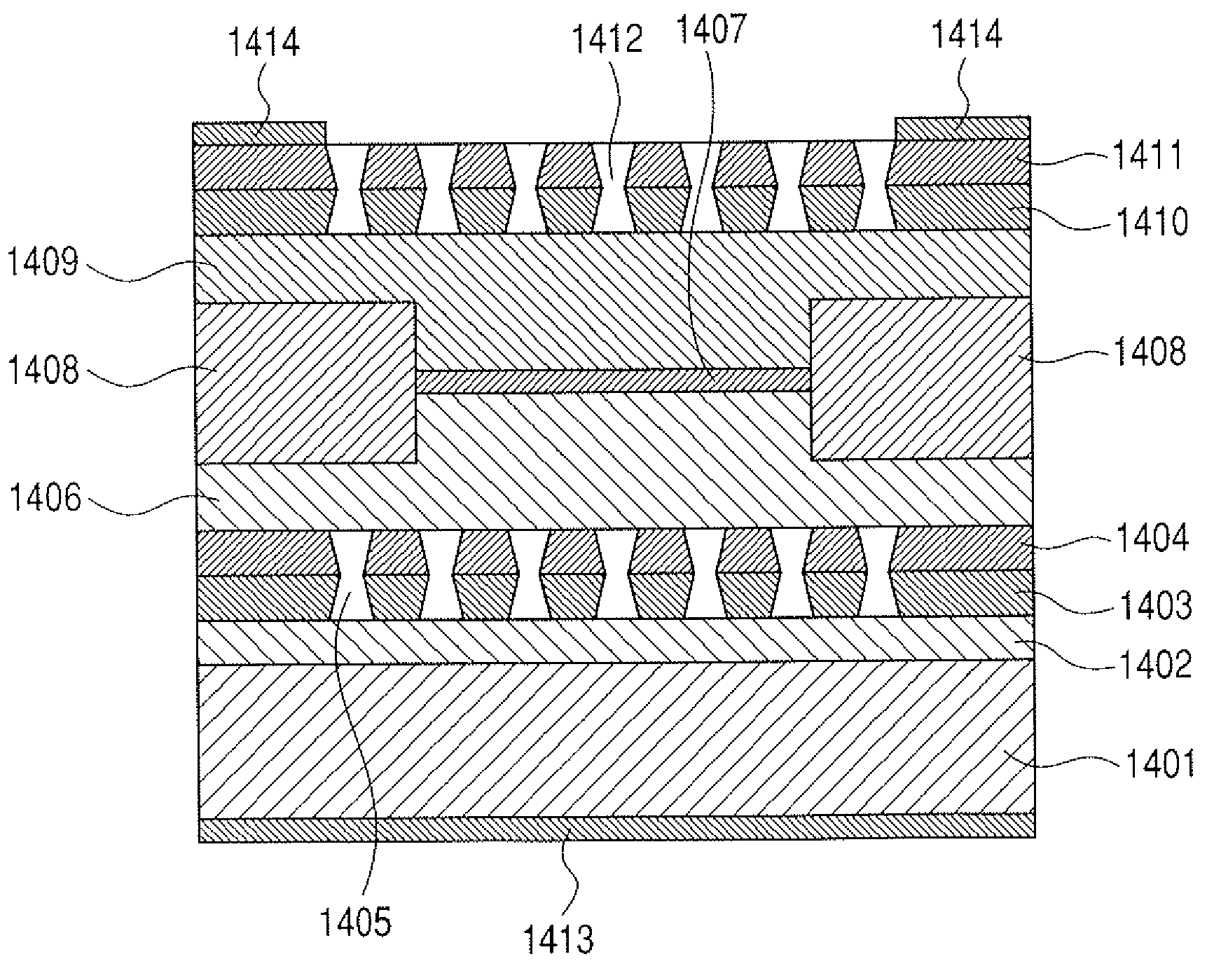
[0247]The vertical cavity surface emitting laser prepared in Example 3 according to the present invention will be described below.
[0248]Since the configuration and the materials of the vertical cavity surface emitting laser of this example are the same as those of Example 2 except the cavity reflectors, only the cavity reflectors of this example will be described below.
[0249]FIGS. 12A and 12B are schematic views of the photonic crystal reflector of Example 3.
[0250]FIG. 12A is a schematic cross sectional view taken along a direction perpendicular to the surface of the photonic crystal. FIG. 12B is a schematic plan view as viewed in the direction perpendicular to the surface of the photonic crystal.
[0251]In this Example, the two reflectors are identical except the thicknesses of the reflectors. Therefore, only the upper cavity reflector in FIGS. 12A and 12B will be described below.
[0252]Referring to FIG. 12A, the layers 1201 through 1204 are made of AlxGa(1-x)As with the value of x va...
PUM
 Abstract
Description
Claims
Application Information