Chemical mechanical polishing process

a mechanical polishing and chemical technology, applied in the direction of chemical apparatus and processes, surface treatment compositions, polishing compositions with abrasives, etc., can solve the problems of parasitic devices formed by the combined layer of neighboring devices, and the failure of attempts to remove residues by continuing polishing, so as to reduce the polishing rate

Active Publication Date: 2007-08-30
MACRONIX INT CO LTD
View PDF6 Cites 4 Cited by
  • Summary
  • Abstract
  • Description
  • Claims
  • Application Information

AI Technical Summary

Benefits of technology

[0015] In particular embodiments, the first dielectric layer is a pad oxide layer and typically the second dielectric layer is a nitride layer. Thus in some embodiments, the first dielectric liner layer is an oxide and the second dielectric liner layer is silicon nitride. In some such processes the third dielectric layer comprises an oxide formed by a high-density plasma deposition process.
[0016] While any suitable polishing composition may be used in the first chemical mechanical polishing operation, typically the polishing composition comprises ceria. In some embodiments, the first polishing composition includes an additive that selectively reduces the polishing rate of the second dielectric layer, particularly where that layer is silicon nitride. Likewise, the second polishing composition may be any suitable polishing composition, but in particular embodiments, the second polishing composition also comprises ceria.

Problems solved by technology

The combined layers of neighboring devices can form parasitic devices.
Attempts to remove the residue by continued polishing are typically unsuccessful even after large amounts of the oxide are removed.

Method used


Image

  • Chemical mechanical polishing process
  • Chemical mechanical polishing process
  • Chemical mechanical polishing process

Examples


examples

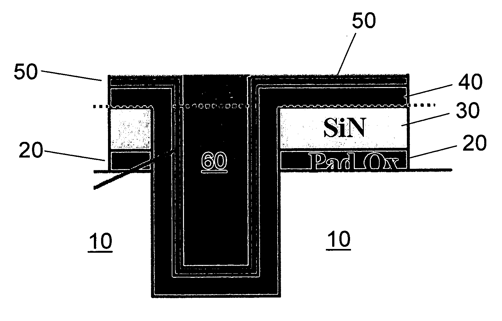
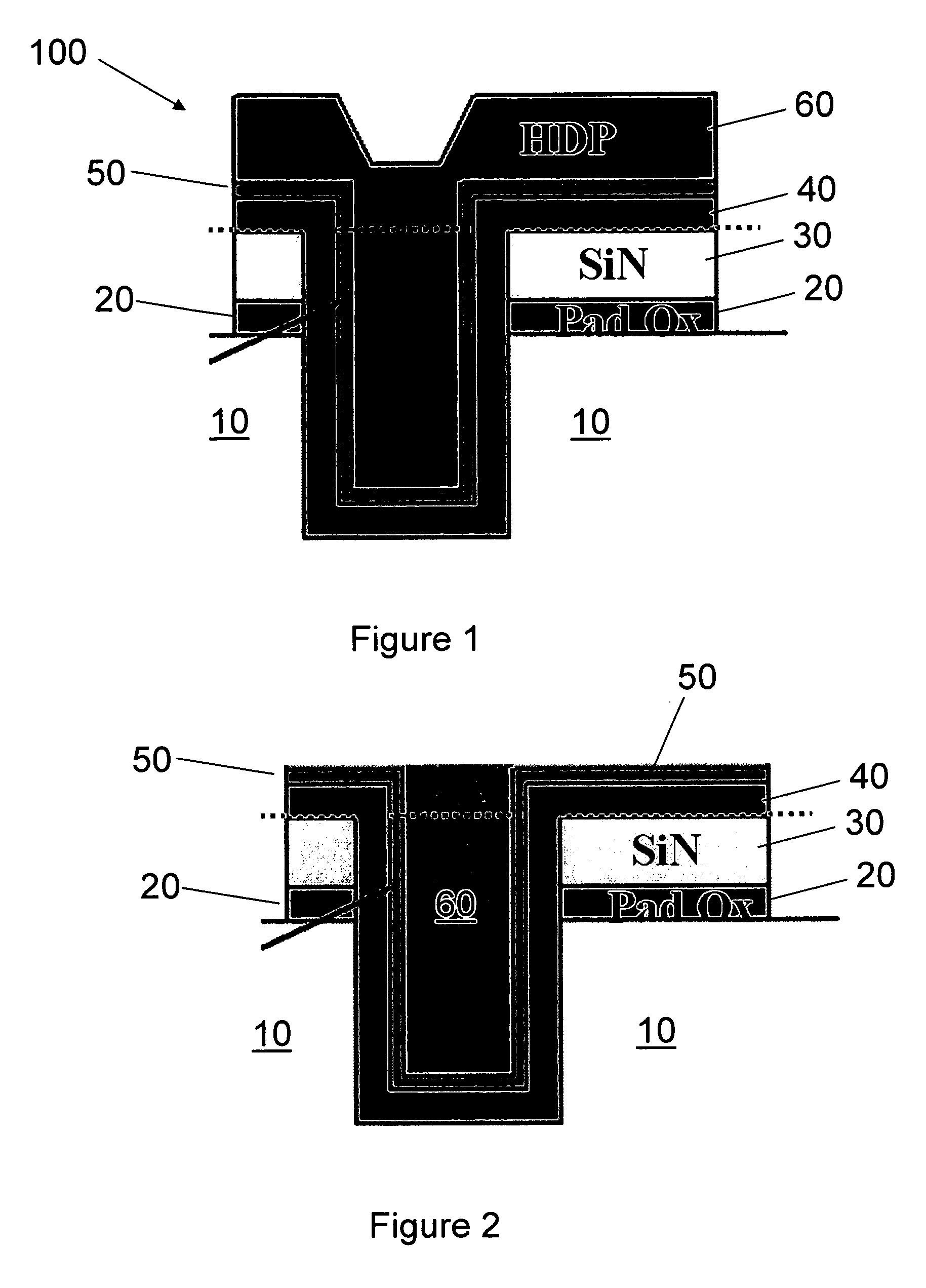
[0040] In Comparative Examples 1-3, a sample structure having trench and diffusion oxide layers as shown in Table I were polished with a ceria slurry. As can be seen in the first column of Table I, different polishing times were used to remove the thin layer above the diffusion SiN layer 30; however, this did not fully remove the second dielectric liner layer.

TABLE IExampleConditionSiO2 A secs +CeO2 B secsTrench Ox(A)Diffusion Ox(A)splitmeanrangeMaxMinmeanrangeMaxMinComparative4506348461542671157714063Example 1A +(B − 10)Comparative444946945954126811271270Example 2A + (B)Comparative431171445583844651231230Example 3A +(B + 10)

[0041]

TABLE IIPolishingResidue thicknessReworkExampleTime(A)TimeComparative45 secResidue (min = 0: max = 100),Rw 7 secExample Aaverage = 101Comparative50 secResidue (min = 0: max = 100),Rw 7 secExample Baverage = 54Comparative55 secResidue (min = 0: max100),Rw 7 secExample Caverage = 70Comparative40 secResidue (min = 0: max = 109),Rw 7 secExample Daverage = 79...


PUM

PropertyMeasurementUnit
flatnessaaaaaaaaaa
flatnessaaaaaaaaaa
widthaaaaaaaaaa

Abstract

A chemical mechanical polishing method is disclosed. The method includes forming a film on a wafer having at least one trench structure thereon; polishing the surface of the film by providing a polishing composition to provide a first polished surface; rinsing the first polished surface with a rinse composition to provide a rinsed surface; and polishing the rinsed surface by providing a second polishing composition to provide a second polished surface.

Description

BACKGROUND [0001] 1. Field of the Invention [0002] Embodiments of the invention relate to methods of chemical mechanical polishing and related device structures. [0003] 2. Background of the Invention [0004] Reductions in semiconductor device dimensions provide higher densities and improved performance for integrated circuits. In many integrated electronic devices, millions of discrete elements, such as transistors, resistors and capacitors are built in close proximity and integrated onto a single device. The combined layers of neighboring devices can form parasitic devices. Thus, one of the important initial steps in the fabrication of semiconductor devices is to electrically isolate adjacent electronic devices on a common substrate. [0005] One technique for forming isolation structures is referred to as the shallow trench isolation (STI) process. To form shallow trench isolation structures a thin pad oxide is first grown on a semiconductor substrate. Thereafter a thin silicon nitri...

Claims


Application Information

Patent Timeline
Patent Type & Authority Applications(United States)
IPC IPC(8): H01L21/302H01L21/461C03C15/00
CPCC09G1/02H01L21/31053H01L21/02065
Inventor FU CHEN, CHUNHUNG, YUNG TAIYANG, YUN CHI
Owner MACRONIX INT CO LTD
Why Eureka
Try Eureka