NOR flash memory device and preparation method thereof

A flash memory device and control gate technology, applied in semiconductor devices, electric solid state devices, electrical components, etc., can solve the problems of breakdown, leakage of NOR flash memory devices, etc., to avoid leakage or breakdown, increase thickness, and reduce polishing rate. Effect

Active Publication Date: 2019-10-15
GIGADEVICE SEMICON SHANGHAI INC +1
View PDF4 Cites 0 Cited by
  • Summary
  • Abstract
  • Description
  • Claims
  • Application Information

AI Technical Summary

Problems solved by technology

[0005] The invention provides a NOR flash memory device and a preparation method thereof, in order to achieve the purpose of improving the reliability of the NOR flash memory device, and solve the problem of leakage or breakdown of the NOR flash memory device caused by the thin floating gate layer

Method used


Image

  • NOR flash memory device and preparation method thereof
  • NOR flash memory device and preparation method thereof
  • NOR flash memory device and preparation method thereof

Examples


Embodiment 1

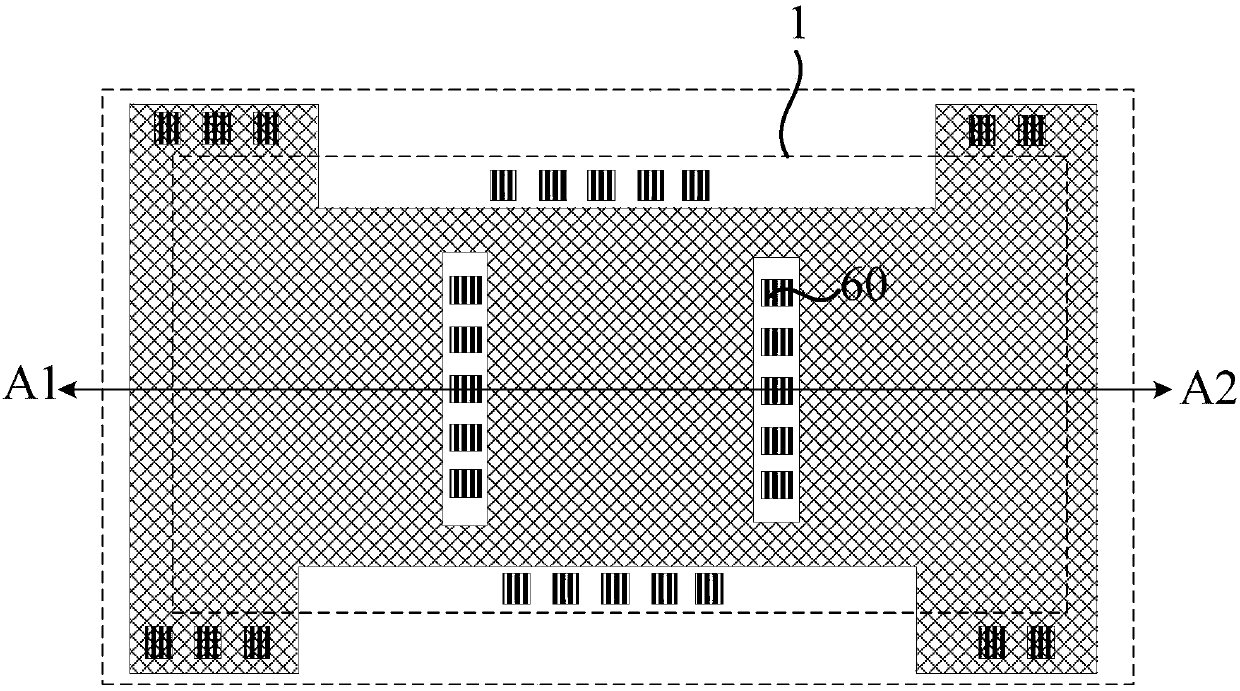
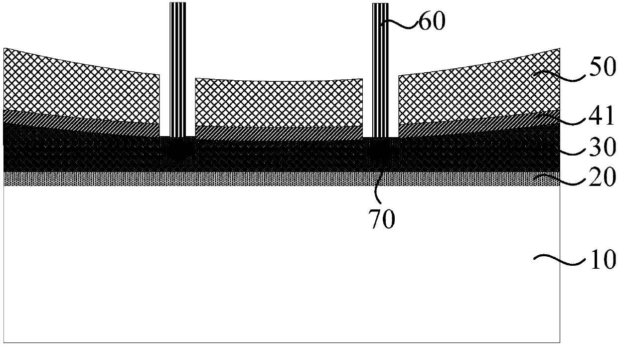
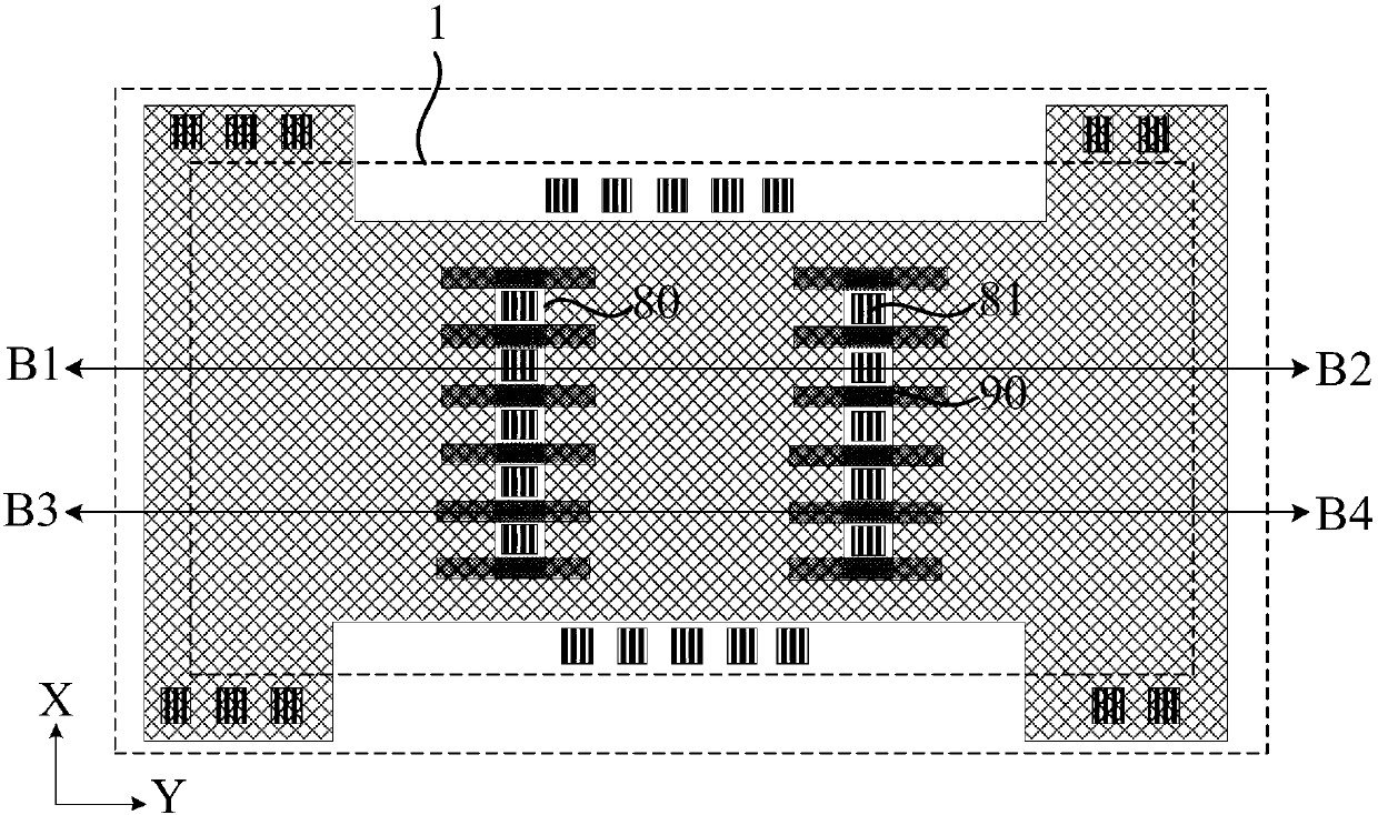
[0042] image 3 It is a schematic top view structure diagram of a NOR flash memory device provided by Embodiment 1 of the present invention. Figure 4 yes image 3 Schematic diagram of the cross-sectional structure along B1-B2. Figure 5 yes image 3 Schematic diagram of the cross-sectional structure along B3-B4. see Figure 3-Figure 5 The NOR flash memory device provided by Embodiment 1 of the present invention includes a substrate 10, a tunnel oxide layer 20, a floating gate layer 30, a dielectric layer 40, and a control gate layer 50 stacked in sequence; at least one through the control gate layer 50 and the dielectric layer The floating gate via hole 80 of the electrical layer 40, the floating gate via hole 80 is located in the active area 1, and is used to expose the floating gate layer 30 to lead out the floating gate electrode 81; at least one active area blocking structure 90, the active area The region barrier structure 90 is disposed between the substrate 10 and...

Embodiment 2

[0080] Figure 11 It is a flow chart of a method for preparing a NOR flash memory device provided in Embodiment 2 of the present invention. Figure 12-Figure 17 It is a structural diagram corresponding to a manufacturing method of a NOR flash memory device provided in Embodiment 2 of the present invention. It should be noted, Figure 13-Figure 15 is the section along the active region barrier structure (see image 3 B3-B4) in the structure diagram of the NOR flash memory device obtained, Figure 16 and Figure 17 is along the cross-section that does not pass through the active region barrier structure (see image 3 Schematic diagram of the NOR flash memory device structure obtained in B1-B2).

[0081] see Figure 11 , the preparation method of the NOR flash memory device provided by the present invention, comprising:

[0082] S10: providing a substrate.

[0083] S20: forming at least one active region blocking structure on the substrate to define an opening area for fo...


PUM


Abstract

The invention discloses an NOR flash memory device and a preparation method thereof. The NOR flash memory device comprises a substrate, a tunneling oxide layer, a floating gate layer, a dielectric layer and a control gate layer, which are stacked up in sequence; at least one floating gate via hole running through the control gate layer and the dielectric layer, wherein the floating gate via hole is arranged in an active region and is used for exposing the floating gate layer to lead out a floating gate electrode; and at least one active region blocking structure, which is arranged between thesubstrate and the dielectric layer and is used for reducing wear of the floating gate layer exposed by the floating gate via hole in the chemical mechanical polishing process of the floating gate layer. According to the technical scheme, by adding the active region blocking structure, polishing rate of the chemical mechanical polishing process for the floating gate layer around can be effectivelyreduced, the thickness of the floating gate layer around is increased, the phenomenon leakage or breakdown of the NOR flash memory device due to too thin floating gate layer can be prevented, and reliability of the NOR flash memory device is improved.

Description

technical field [0001] Embodiments of the present invention relate to semiconductor device technology, and in particular to a NOR flash memory device and a manufacturing method thereof. Background technique [0002] For the floating gate (Floating Gate, FG) NOR flash memory device manufactured by the traditional process of 90 / 65nm node and below, in order to increase the capacitance per unit area of ​​the high withstand voltage capacitor, improve the utilization rate of the chip area, and reduce the cost, a stacking method will be introduced. The oxide layer-nitride layer-oxide layer (Oxide-Nitride-Oxide, ONO) capacitor of the first layer is used in a high-voltage charge pump. [0003] figure 1 It is a top view structure diagram of an ONO capacitor in the prior art. figure 2 yes figure 1 Schematic diagram of the cross-sectional structure along A1-A2. see figure 1 and figure 2 The ONO capacitor is composed of a silicon substrate 10 - a tunnel oxide (Tunnel Oxide, TO) ...

Claims


Application Information

Patent Timeline
Patent Type & Authority Applications(China)
IPC IPC(8): H01L27/115H01L27/11517
CPCH10B41/00H10B69/00
Inventor 熊涛刘钊许毅胜舒清明
Owner GIGADEVICE SEMICON SHANGHAI INC
Why Eureka
Try Eureka