

Method for producing a substrate by germanium condensation
a technology of germanium condensation and substrate, which is applied in the direction of basic electric elements, semiconductor/solid-state device manufacturing, electrical equipment, etc., can solve the problems of unwieldy technique for producing localized goi substrates, high cost of technology, and difficult to achieve nmosfet transistors, etc., and achieves the effect of easy implementation
- Summary
- Abstract
- Description
- Claims
- Application Information
AI Technical Summary
Benefits of technology
Problems solved by technology
Method used
Image

Examples
Embodiment Construction
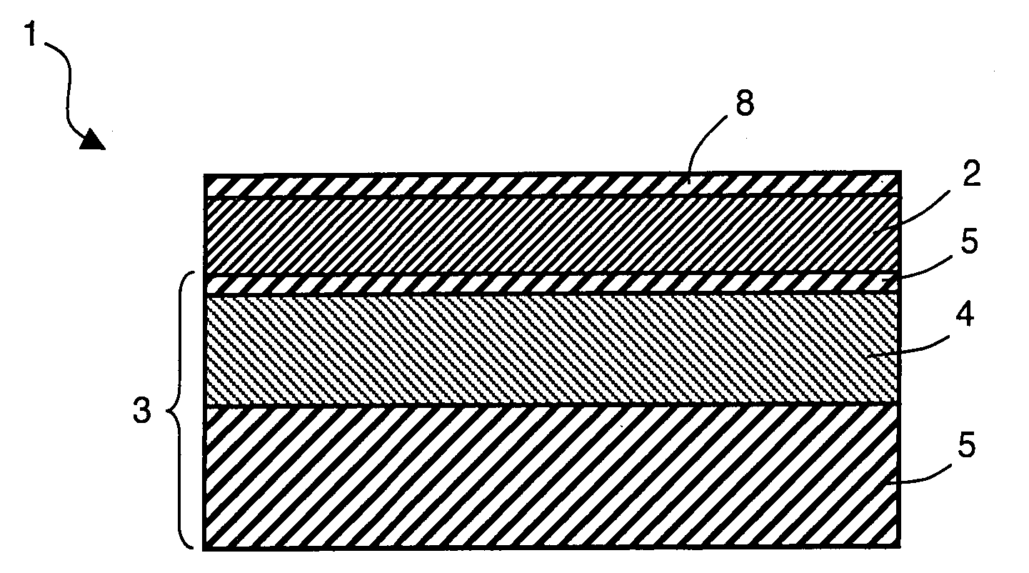
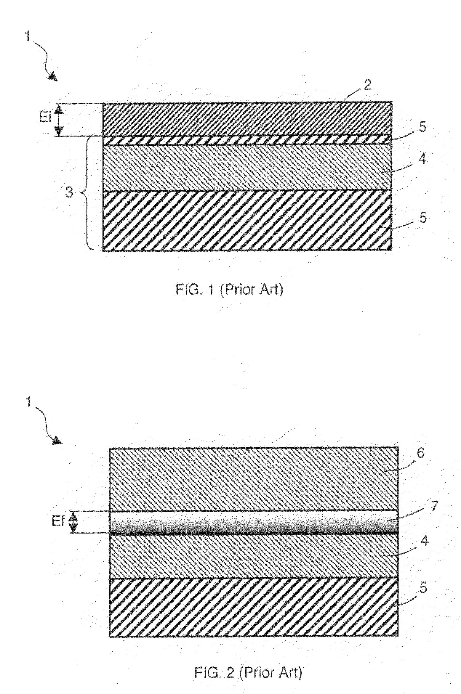
[0024]With reference to FIGS. 3 to 5, the fabrication method is designed to produce a silicon and germanium on insulator (SGOI) or a germanium on insulator (GOI) substrate 1, i.e. a substrate comprising a silicon and germanium compound Si1-XfGeXf on insulator. The final germanium concentration Xf is strictly comprised between 0 and 1 for a SGOI substrate, and the final germanium concentration Xf is equal to 1 for a GOI substrate.
[0025]The fabrication method first comprises formation of the substrate on insulator 3 and formation, for example by epitaxy, of the Si1-XiGeXi silicon and germanium alloy layer 2 (FIG. 1). The method then comprises thermal oxidation treatment of the silicon, preferably performed at high temperature and notably consisting in injecting an oxidizing gas into for example a chamber in which the fabrication method of the substrate 1 is performed.
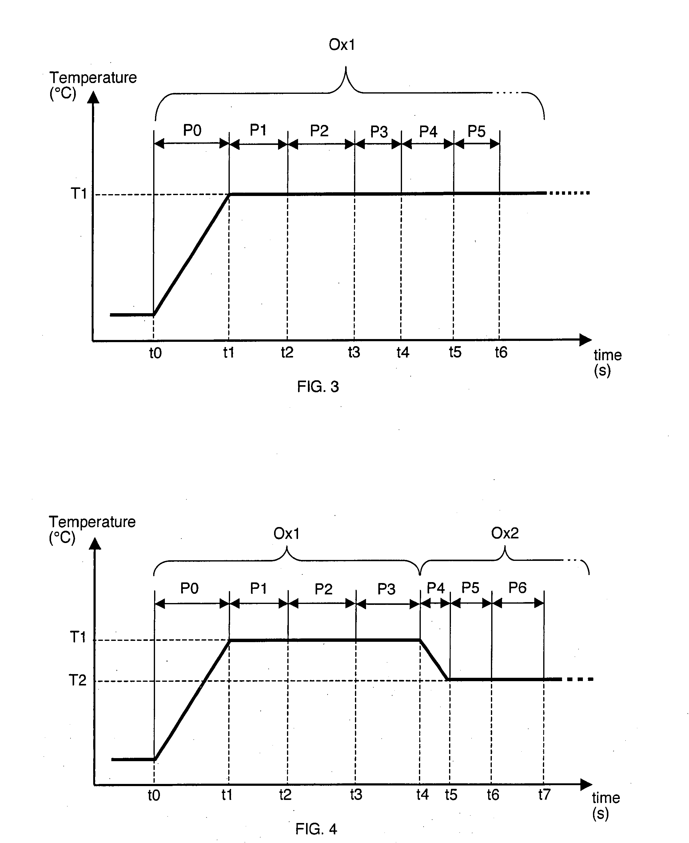
[0026]In FIG. 3, a first thermal oxidation step Ox1 of the silicon of the layer 2 comprises a prior temperature increas...
PUM
| Property | Measurement | Unit |
|---|---|---|
| temperature | aaaaa | aaaaa |
| temperature | aaaaa | aaaaa |
| thickness | aaaaa | aaaaa |
Abstract
Description
Claims
Application Information