Liquid crystal display device

Active Publication Date: 2007-09-13
SHARP KK
View PDF8 Cites 21 Cited by
  • Summary
  • Abstract
  • Description
  • Claims
  • Application Information

AI Technical Summary

Benefits of technology

[0038] According to the invention, the liquid crystal display device

Problems solved by technology

However, the TN mode liquid crystal display device has defects that a viewing angle characteristic is poor and when a screen is viewed from an oblique direction, the contrast and hue are remarkably changed.
However, in the liquid crystal display device shown in FIG. 23 and FIG. 24, since the control capacitance electrodes 133 and 134 are formed of metal layers which are the same layers as the source electrode 122 and the drain electrode 121 and shield t

Method used


Image

  • Liquid crystal display device
  • Liquid crystal display device
  • Liquid crystal display device

Examples


Example

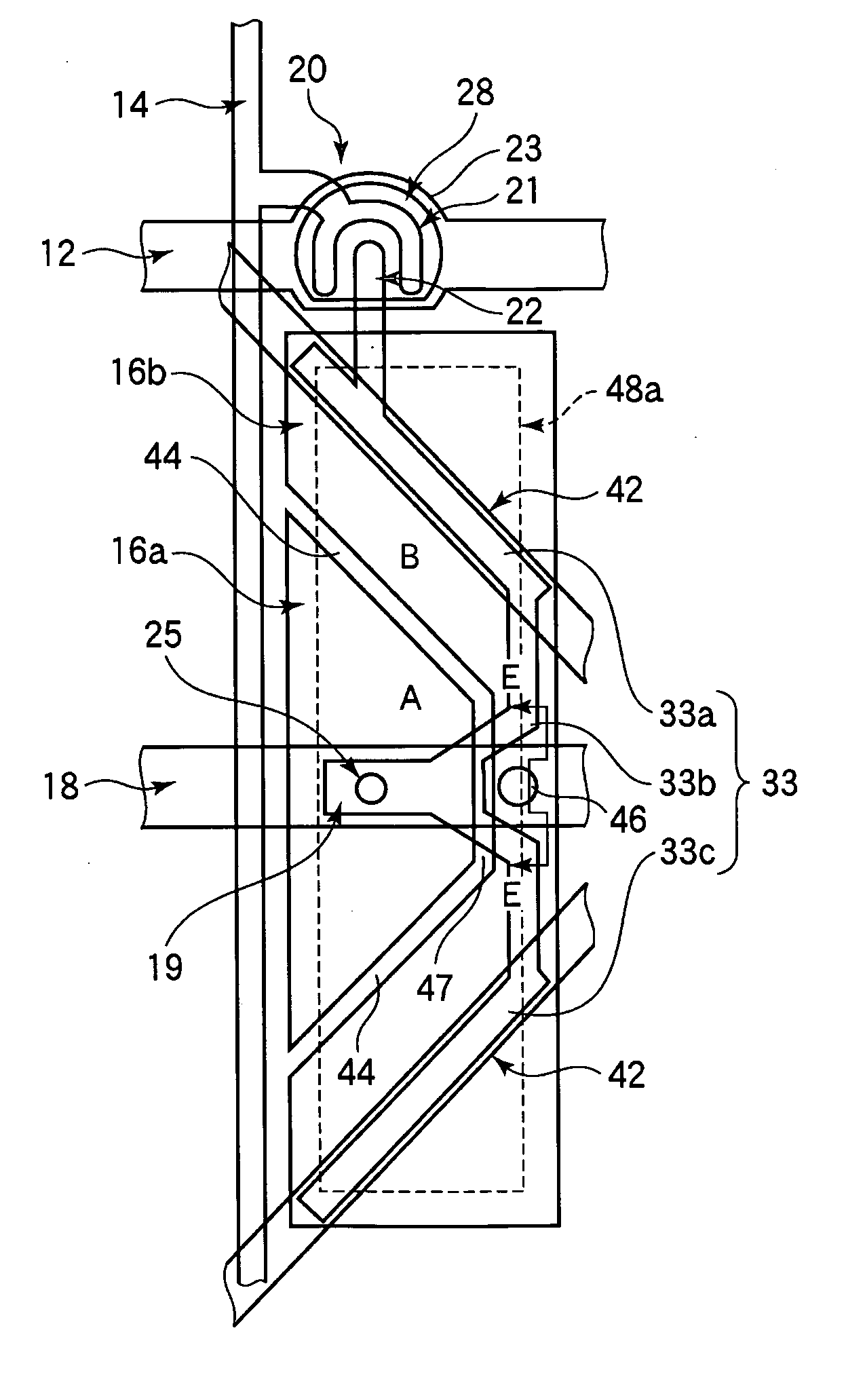
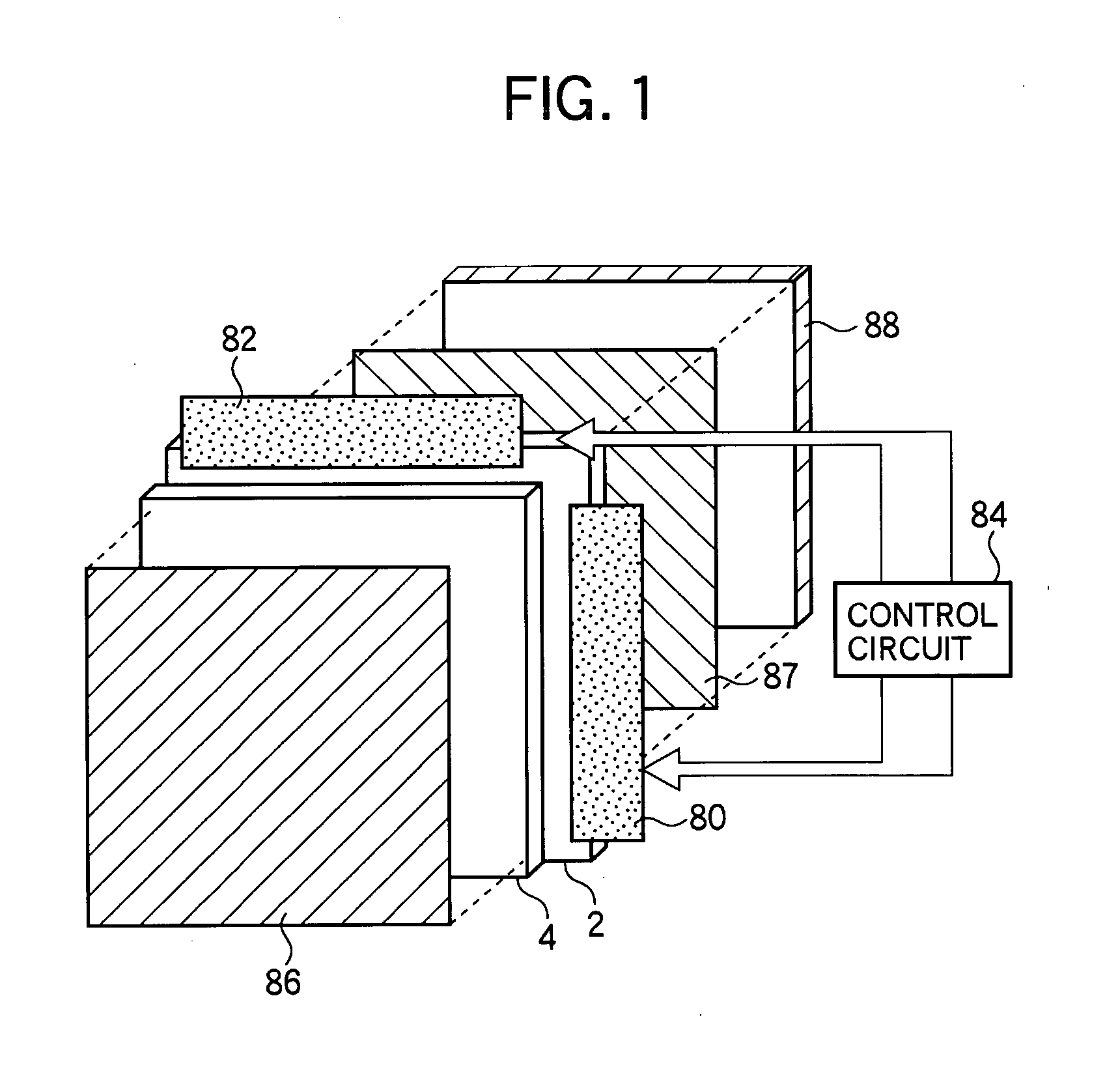
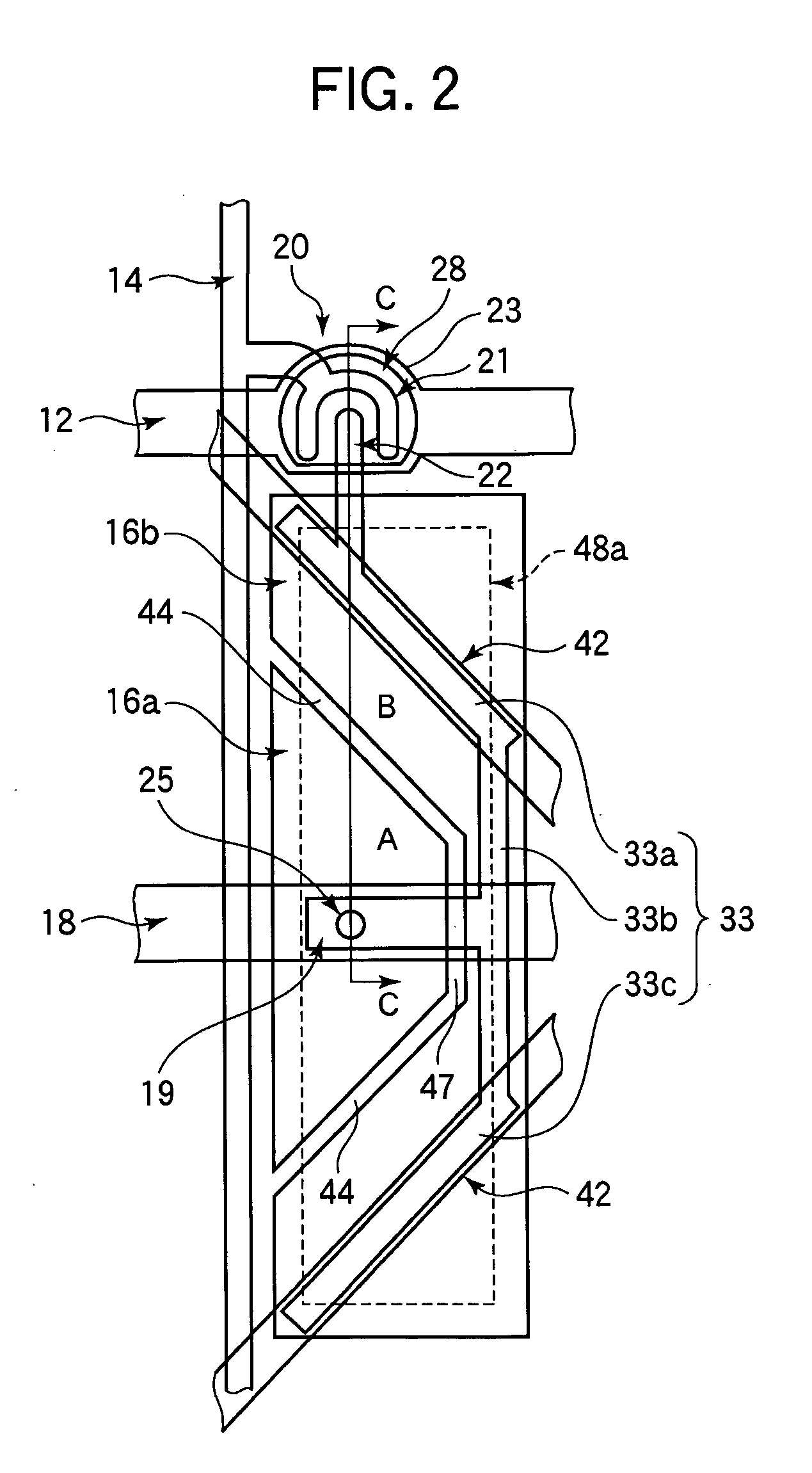
[0063] A liquid crystal display device according to a first embodiment of the invention will be described with reference to FIGS. 1 to 7. FIG. 1 shows a rough structure of the liquid crystal display device according to this embodiment. As shown in FIG. 1, the liquid crystal display device includes a TFT substrate 2 on which gate bus lines and drain bus lines are formed to cross each other through an insulating film, and on which a TFT and a pixel electrode are formed for each pixel. Besides, the liquid crystal display device includes an opposite substrate 4 on which a CF and a common electrode are formed and which is disposed to be opposite to the TFT substrate 2, and a vertically aligned liquid crystal 6 (not shown in FIG. 1) sealed between both the substrates 2 and 4 and having negative dielectric anisotropy.

[0064] The TFT substrate 2 is connected with a gate bus line drive circuit 80 in which a driver IC to drive the plural gate bus lines is mounted and a drain bus line drive ci...

Example

Second Embodiment

[0094] Next, a liquid crystal display device according to a second embodiment of the invention will be described with reference to FIGS. 8 to 14F. FIG. 8 shows a structure of a B pixel (pixel in which a blue CF resin layer is formed) of the liquid crystal display device of this embodiment, and FIG. 9 shows a structure of an R pixel or a G pixel (pixel in which a red or a green CF resin layer is respectively formed) of the liquid crystal display device of this embodiment. FIG. 10A shows a sectional structure of the liquid crystal display device cut along line D-D of FIG. 8, and FIG. 10B shows a sectional structure of the liquid crystal display device cut along line E-E of FIG. 9. FIG. 11A and FIG. 11B show sectional structures of an opposite substrate 4 before being bonded to the TFT substrate 2. FIG. 11A shows the sectional structure of the opposite substrate 4 cut at the same position as FIG. 10A, and FIG. 11B shows the sectional structure of the opposite substrat...


PUM


Abstract

There is provided an MVA type liquid crystal display device having high brightness and excellent display quality. The liquid crystal display device includes a pair of substrates disposed to be opposite to each other, a liquid crystal sealed between the pair of substrates, plural pixel areas each including a pixel electrode 16a formed on one of the substrates and a pixel electrode 16b separated from the pixel electrode 16a, a TFT 20 disposed in each of the pixel areas and including a source electrode 22 electrically connected to the pixel electrode 16a, a linear projection 42 formed on the other substrate and to regulate alignment of the liquid crystal, and a control capacitance section to capacity couple the source electrode 22 and the pixel electrode 16b and including a control capacitance electrode 33 which is electrically connected to the source electrode 22, is opposite to at least part of the pixel electrode 16b through an insulating film, and at least part of which is disposed to overlap with the linear projection 42 when viewed perpendicularly to a substrate surface and extends along the linear projection 42.

Description

BACKGROUND OF THE INVENTION [0001] 1. Field of the Invention [0002] The present invention relates to an MVA (Multi-domain Vertical Alignment) type liquid crystal display device in which one pixel includes plural alignment areas different from each other in the alignment direction of liquid crystal molecules, and particularly to a liquid crystal display device in which a pixel area is divided into plural sub-pixels. [0003] 2. Description of the Related Art [0004] A liquid crystal display device is thin and lightweight as compared with a CRT (Cathode Ray Tube), and has merits that it can be driven by low voltage and its electric power consumption is small. Thus, the liquid crystal display device is used for various electronic devices such as a notebook PC (personal computer), a PDA (Personal Digital Assistant) and a cellular phone. Especially, an active matrix type liquid crystal display device in which a TFT (Thin Film Transistor) is provided as a switching element for each pixel has...

Claims


Application Information

Patent Timeline
IPC IPC(8): G02F1/1343
CPCG02F1/133707G02F1/13394G02F1/136213G02F1/1393G02F2201/123G02F2001/134345G02F2001/134354G02F2001/136218G02F2001/13396G02F1/13396G02F1/134345G02F1/134354G02F1/136218G02F1/1337
Inventor MISAKI, KATSUNORIFUJIKAWA, TETSUYATAGUCHI, YOSHIHISANAGAOKA, KENICHISAWASAKI, MANABU
Owner SHARP KK
Why Eureka
Try Eureka