Molded high impedance surface

a technology of impedance surface and molding, which is applied in the direction of fixed capacitor details, variable capacitors, fixed capacitors, etc., can solve the problems of inability to drill the via b, most time-consuming and expensive tasks, etc., and achieve the effect of large area and low cos

Inactive Publication Date: 2007-09-13
HRL LAB
View PDF91 Cites 16 Cited by
  • Summary
  • Abstract
  • Description
  • Claims
  • Application Information

AI Technical Summary

Benefits of technology

[0006] The present invention provides a Hi-Z surface that can be produced by injection molding, which permits large areas to be produced rapidly and at a low cost. Additionally, certain embodiments of the structure are also technically superior in that they can be tuned after

Problems solved by technology

Because of its high impedance, the Hi-Z structure can support a finite tangential electric field at its surface, whic

Method used


Image

  • Molded high impedance surface
  • Molded high impedance surface
  • Molded high impedance surface

Examples


Embodiment Construction

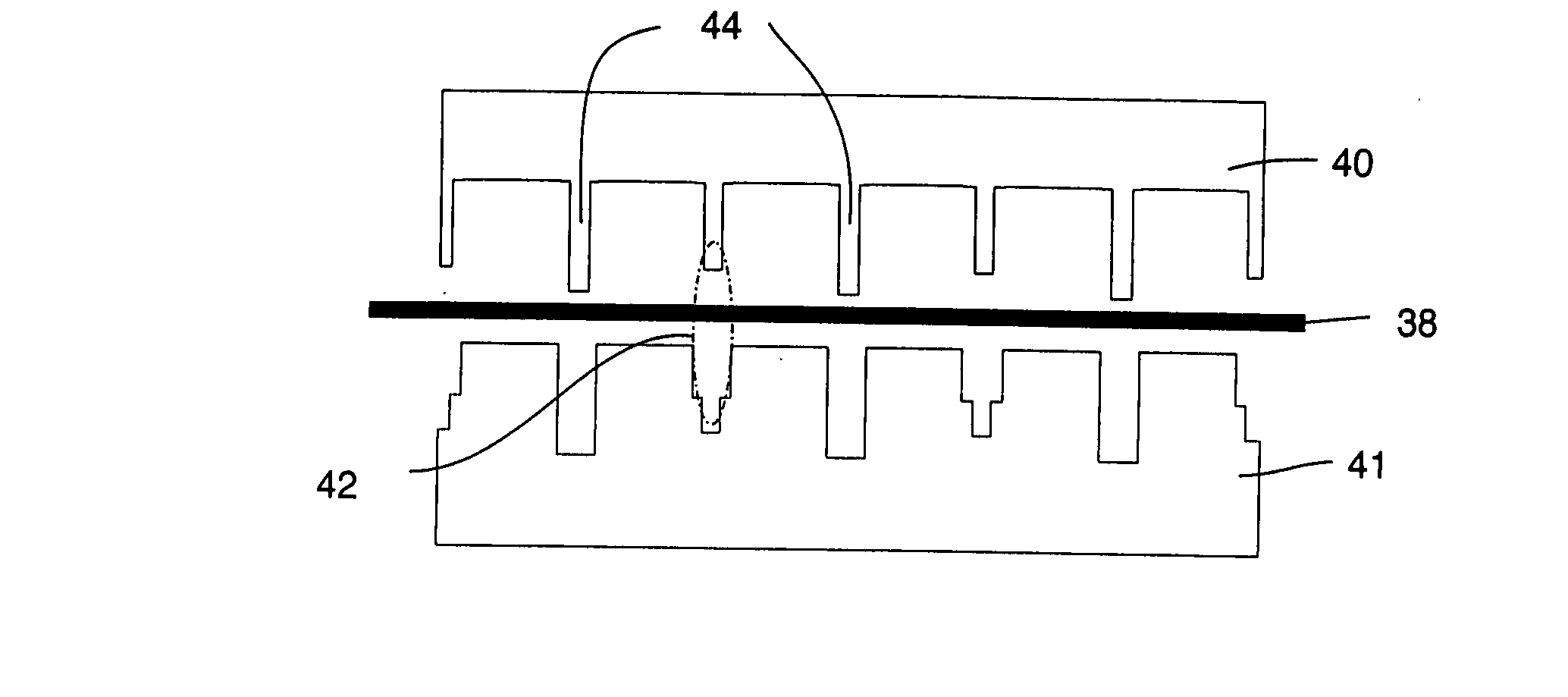
[0022] A preferred embodiment of the present invention will now be described with reference to FIGS. 3(a) and 3(b) and FIGS. 4(a)-4(e). FIG. 3(a) is a cross section view through structure 11 as marked by section line 3(a) noted on FIG. 3(b). FIGS. 4(a)-4(e) are also section views taken along the same section line done for FIG. 3(a) but at later points in the fabrication of the high impedance surface of the present invention.

[0023] In this embodiment a form or structure 11 is fabricated by molding and the form 11 is subsequently plated with metal and the metal is partially removed to define the capacitor structures. The form or structure 11 is preferably made by injection molding, in which a mold is filled with a liquid dielectric material, which then hardens into a solid cast which is removed from the mold. This dielectric material is preferably either a thermoplastic, which is melted and then injected into the mold and allowed to harden, or a thermoset resin, which is mixed in liq...


PUM


Abstract

A high impedance surface and a method of making same. The surface includes a molded structure having a repeating pattern of holes therein and a repeating pattern of sidewall surfaces, the holes penetrating the structure between first and second major surfaces thereof and the sidewall surfaces joining the first major surface. A metal layer is put on said molded structure, the metal layer being in the holes, covering at least a portion of the second major surface, covering the sidewalls and portions of the first major surface to interconnect the sidewalls with other sidewalls via the metal layer on the second major surface and in the holes.

Description

TECHNICAL FIELD [0001] This invention improves upon current techniques for manufacturing high impedance surfaces which surfaces are also known as resonant textured ground planes or a “Hi-Z” surfaces and which surfaces are presently made using printed circuit board techniques. The present invention provides new methods of manufacturing such surfaces based on molding and / or related techniques, and also provides several structures that are manufacturable using these techniques. The invention allows Hi-Z surfaces to be mass-produced more rapidly and at a lower cost than the prior art techniques, which primarily involve printed circuit board technology. This invention also provides a Hi-Z structure in which the capacitors are vertical, instead of horizontal, so that they may be trimmed after manufacturing, for tuning purposes. BACKGROUND OF THE INVENTION [0002] Recently, a new kind of electromagnetic ground plane has been developed which is known as a high-impedance or Hi-Z surface. See ...

Claims


Application Information

Patent Timeline
IPC IPC(8): H01G7/00
CPCH01G4/005H01G4/38H05K1/144H05K1/162H05K3/045H05K3/107H05K2203/0455H05K3/426H05K2201/041H05K2201/09036H05K2201/09045H05K2201/09118H05K2201/09981H05K3/3436
Inventor SIEVENPIPER, DANIEL F.PIKULSKI, JOSEPH L.SCHAFFNER, JAMES H.HSU, TSUNG-YUAN
Owner HRL LAB
Why Eureka
Try Eureka