Interconnect structure with a barrier-redundancy feature

a technology of interconnection structure and redundancy feature, which is applied in the direction of semiconductor devices, semiconductor/solid-state device details, electrical apparatus, etc., can solve the problems of shortening the accumulation time before an open circuit, circuit to open, and undesirable void accumulation

Active Publication Date: 2007-09-13
AURIGA INNOVATIONS INC
View PDF13 Cites 30 Cited by
  • Summary
  • Abstract
  • Description
  • Claims
  • Application Information

AI Technical Summary

Benefits of technology

[0009] The present invention provides an interconnect structure that includes a barrier-redundancy feature which is capable of avoiding a sudden open circuit after an electromigration (EM) failure as well as a method of forming the same. In accordance with the present invention, the barrier-redundancy f

Problems solved by technology

This void accumulation is undesirable since it will slow down signal transmission speed because of increasing electrical resistivity and eventually can cause the circuit to open as soon as the void size covers the entire contact area.
The above mentioned failure results from a current density divergence at the contact area and is attributed to a phenomenon of electromigration (EM) failure inside the conductive interconnect.
As the feature size of current se

Method used


Image

  • Interconnect structure with a barrier-redundancy feature
  • Interconnect structure with a barrier-redundancy feature
  • Interconnect structure with a barrier-redundancy feature

Examples


Embodiment Construction

[0031] The present invention, which provides an interconnect structure including a barrier-redundancy feature that avoids a sudden open circuit after an electromigration failure has been detected by a monitoring device and a method of fabricating the same, will now be described in greater detail by referring to the following description and drawings that accompany the present application. The drawings of the present application, which are referred to herein below in greater detail, are provided for illustrative purposes and, as such, they are not drawn to scale.

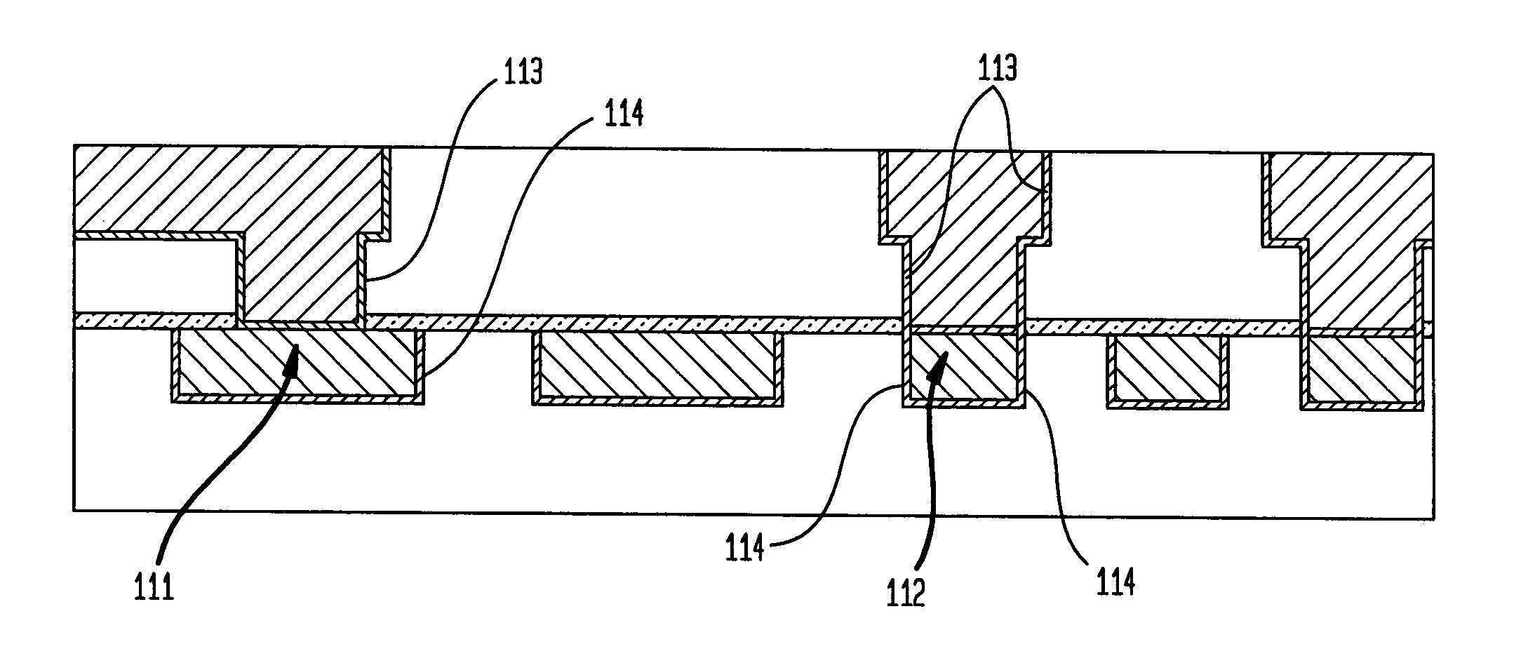
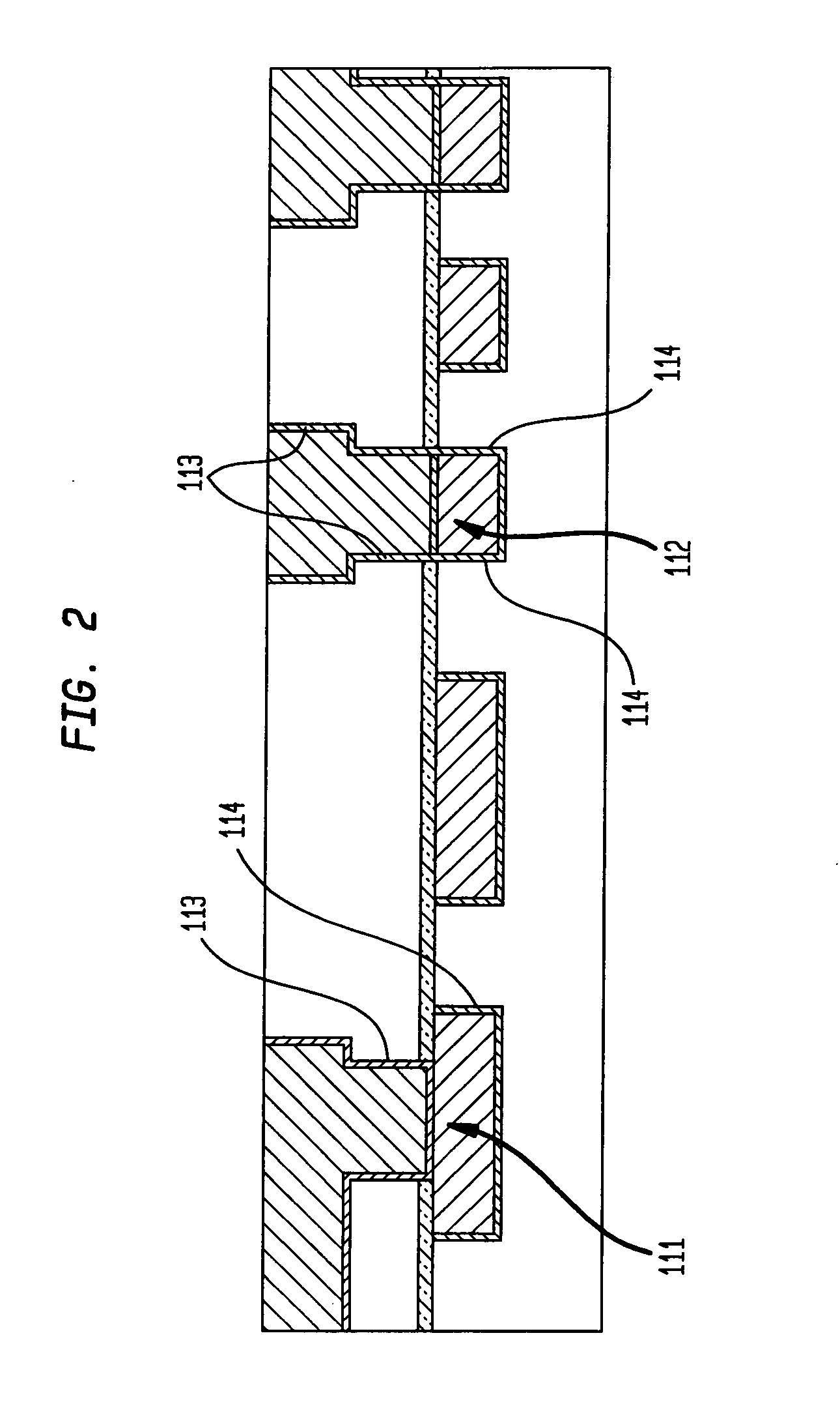
[0032] Before describing the basic process flow, it is noted that the following description illustrates a preferred embodiment of the present invention in which the barrier-redundancy feature is located with a wide line of the interconnect structure.

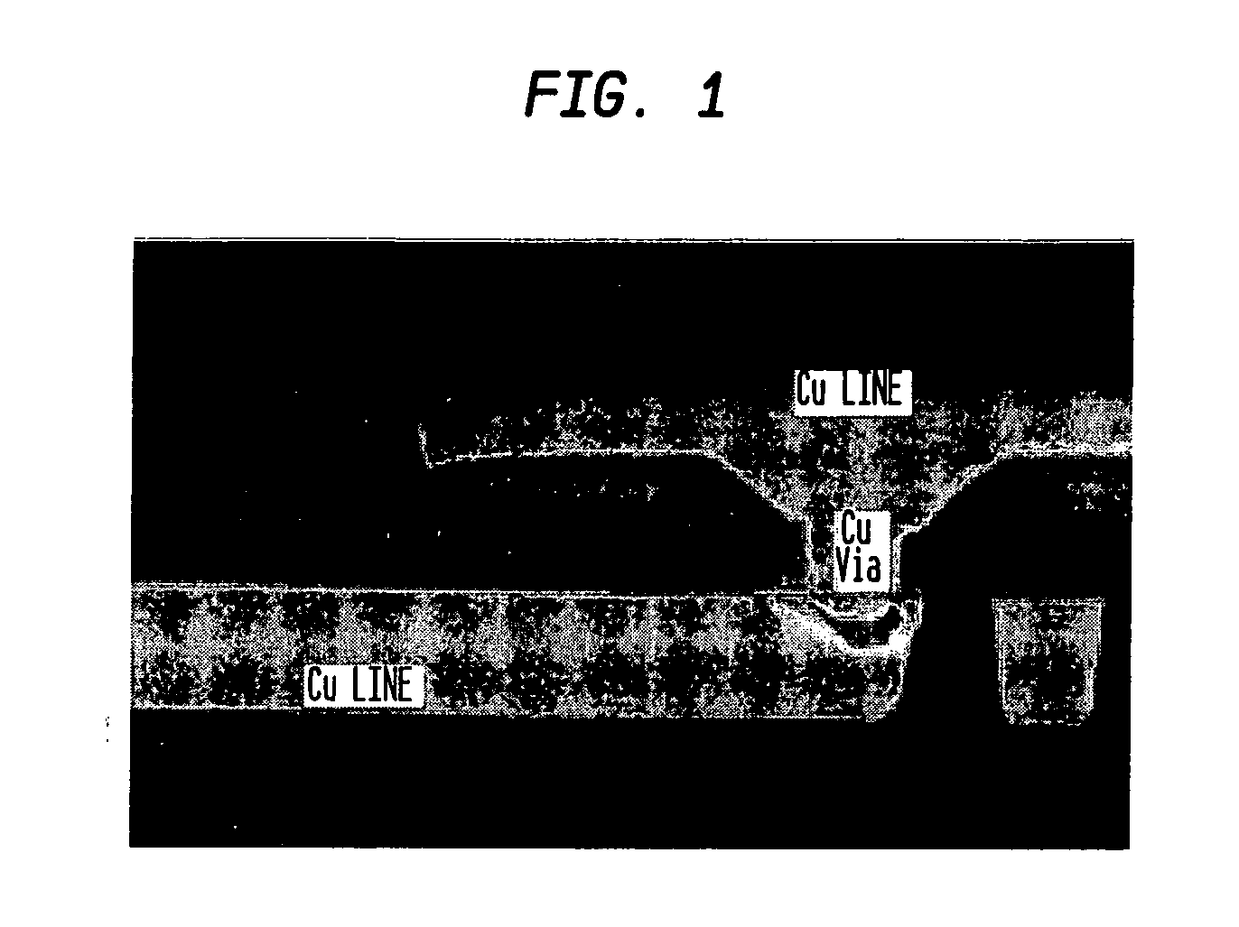
[0033] The process flow of the present invention begins with providing the initial interconnect structure 10 shown in FIG. 4A. Specifically, the initial interconnect structure 1...


PUM


Abstract

An interconnect structure that includes a barrier-redundancy feature which is capable of avoiding a sudden open circuit after an electromigration (EM) failure as well as a method of forming the same are provided. In accordance with the present invention, the barrier-redundancy feature is located within preselected locations within the interconnect structure including in a wide line region, a thin line region or any combination thereof. The barrier-redundancy feature includes an electrical conductive material located between, and in contact with, a conductive line diffusion barrier of a conductive line and a via diffusion barrier of an overlying via. The presence of the inventive barrier-redundancy feature creates an electrical path between the via diffusion barrier along the sidewalls of the via and the conductive line diffusion barrier along the sidewalls of the conductive line. This electrical path generated by the inventive barrier-redundancy feature can avoid a sudden open circuit resulting from EM failure at the bottom of the via. The presence of the inventive barrier-redundancy feature within an interconnect structure provides sufficient time for chip replacement or system operation.

Description

FIELD OF THE INVENTION [0001] The present invention relates to a semiconductor structure and a method of fabricating the same. More particularly, the present invention relates to an interconnect structure including a barrier-redundancy feature that avoids a sudden open circuit after an electromigration failure has been detected by a monitoring device. The present invention also relates to a method of fabricating an interconnect structure which includes the above-mentioned feature. BACKGROUND OF THE INVENTION [0002] Generally, semiconductor devices include a plurality of circuits which form an integrated circuit fabricated on a semiconductor substrate. A complex network of signal paths will normally be routed to connect the circuit elements distributed on the surface of the substrate. Efficient routing of these signals across the device requires formation of multilevel or multilayered schemes, such as, for example, single or dual damascene wiring structures. The wiring structure typi...

Claims


Application Information

Patent Timeline
IPC IPC(8): H01L21/4763
CPCH01L21/76849H01L23/53238H01L23/53295H01L2924/0002H01L2924/00
Inventor YANG, CHIH-CHAOHSU, LOUIS L.
Owner AURIGA INNOVATIONS INC
Why Eureka
Try Eureka