Method for reducing defect concentrations in crystals

a technology of defect concentration and crystal structure, applied in the field of crystal structure, can solve the problems of deformation of epitaxial layers, defects can also exist in amorphous, degrade the quality, performance and lifetime of epitaxial layers, etc., and achieve the effect of reducing the concentration of defect defects in crystal structure and reducing the amount of strain

Inactive Publication Date: 2007-02-13
DIAMOND INNOVATIONS INC
View PDF14 Cites 95 Cited by
  • Summary
  • Abstract
  • Description
  • Claims
  • Application Information

AI Technical Summary

Problems solved by technology

Crystal performance in these applications often is limited by the material quality of the crystals, in particular, the concentration of defects.
Defects also introduce strain into crystals, which tends to degrade the quality, performance, and lifetime of epitaxial layers and electronic devices grown on wafers sliced from these crystals Reduction or elimination of these defects during crystal growth can be very difficult, so alternate means would be useful.
Defects can also exist in amorphous materials, such as glasses, plastics, and metals, which may detract from their optical, mechanical, electrical, or visual properties.
Both micro-pipes and dislocations have been strongly linked with device failure and degradation phenomena.
One reason why silicon carbide based devices have not emerged from small niche markets into large scale, high-power applications is the unreliability of devices resulting from substrate defects.
However, applicants are not aware of any currently available method to grow SiC crystals with a micropipe density below 1 cm−2, or SiC crystals of at least 25 mm, at least 50 mm, at least 75 mm, or even at least 100 mm diameter that are entirely free of micropipes.
However, these methods require expensive procedures to be applied one-at-a-time to individual SiC wafers.
Additionally, they do not provide SiC crystals of at least 25 mm, at least 50 mm, at least 75 mm, or at least 100 mm in diameter that are free of micropipes and microvoids through their entire volume.
In the case of gallium nitride, the quality of substrates currently is low, as they are typically prepared by heteroepitaxy on non-GaN substrates, such as, for example, sapphire or silicon carbide.
GaN also tends to grow with substantial concentrations of native defects, such as vacancies, both on Ga and N sites.
The quality of gallium arsenide and indium phosphide wafer substrates is considerably higher than that of SiC or GaN, but the concentration of defects (dislocations, vacancies) is nonetheless sufficiently high to have a deleterious effect on the performance of electronic devices fabricated thereon.
The growth technology is sufficiently mature that significant incremental improvements are unlikely.
These treatments modify the nature, concentration, and distribution of point defects (vacancies, interstitials, substitutional impurities), but these authors provide no teaching about reduction in the concentration of voids, micro- or nanopipes, or dislocations.
The annealing conditions taught by Porowski, et al. have been sufficient to anneal point defects and cause atomic diffusion, but no reduction of threading dislocations, micro- or nano-pipes or voids was demonstrated.
However, no reduction of threading dislocations, micro- or nano-pipes or voids is demonstrated and that vacancies in Si could be aggregated into voids.

Method used


Image

  • Method for reducing defect concentrations in crystals
  • Method for reducing defect concentrations in crystals

Examples


examples

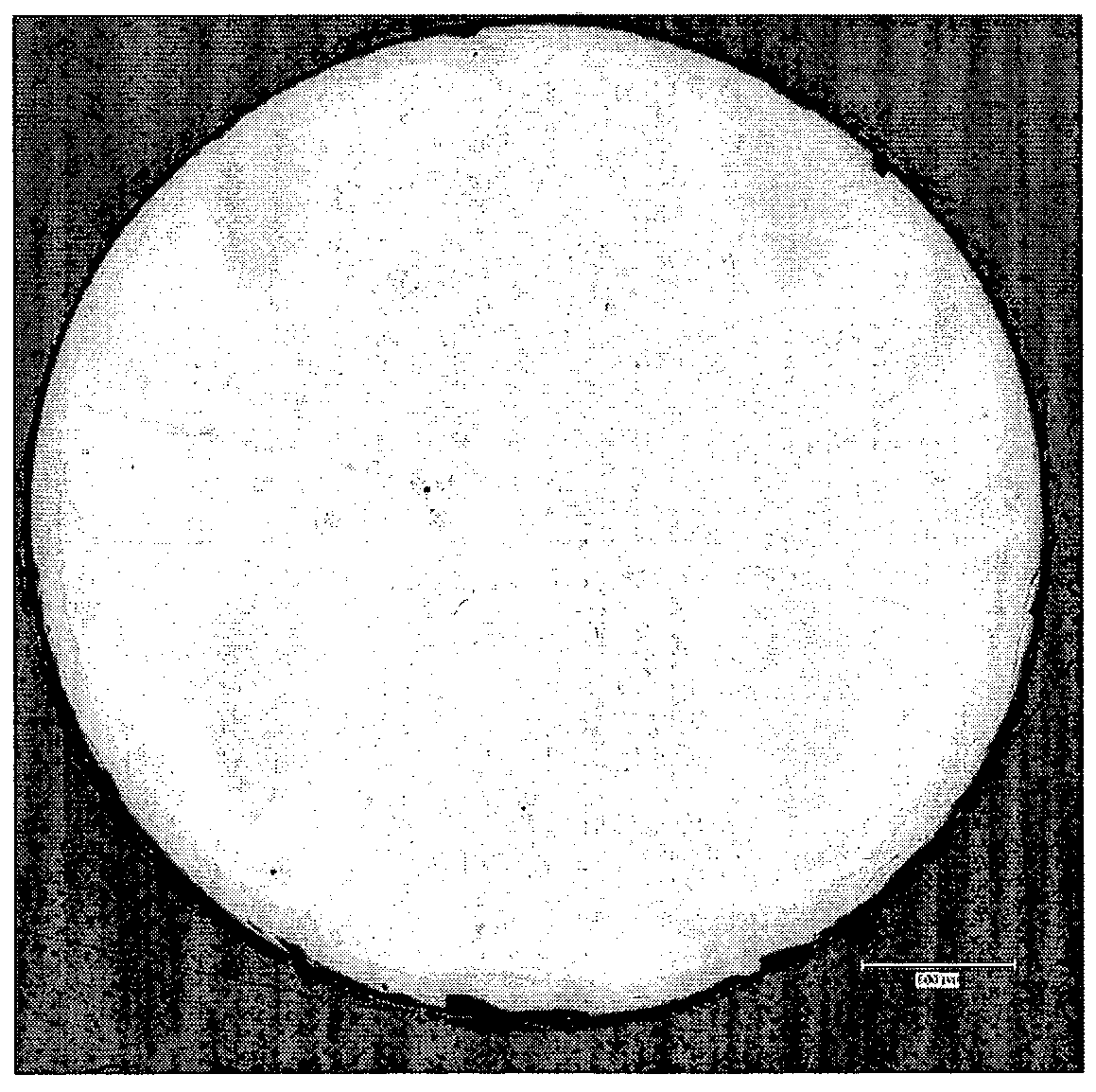
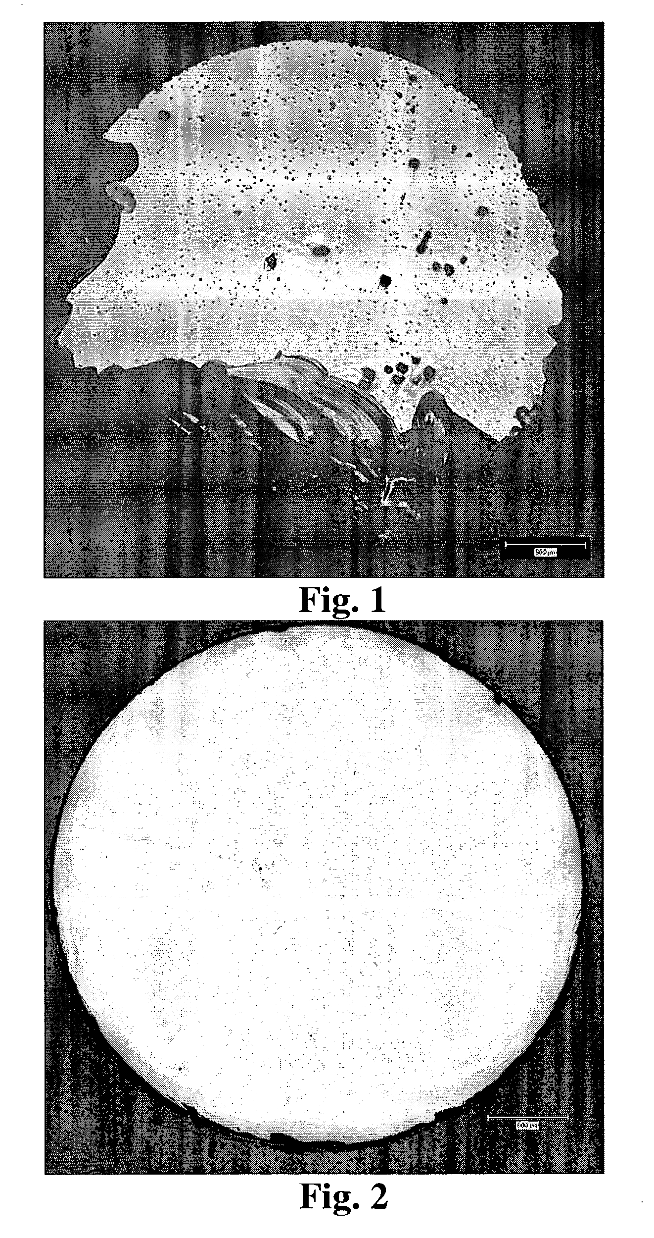
[0040]In the examples, a SiC disk, approximately 3 mm diameter by 1 mm thick, is cut from the end of a 6H—SiC boule that had been grown by conventional physical vapor transport. One surfaces of the SiC disk is finely polished and the concentration of micropipes is characterized by optical microscopy. A dark field photomicrograph of this sample prior to annealing is shown in FIG. 1. The largest dark spots in FIG. 1 are the result of voids present in the SiC boule that are intersected by the slice used to prepare the wafer. The numerous smaller dark spots in FIG. 1 are micropipes, which normally extend throughout the boule.

[0041]The SiC disk is placed inside a die along with NaCl powder and compacted into a pill. The pill is assembled into a cell and placed inside a belt press apparatus. The pill is pressurized to approximately 5.5 GPa and heated to about 1250° C. for about 30 minutes. The cell then is cooled and depressurized and removed from the press. The SiC disk is recovered from...


PUM

PropertyMeasurementUnit
temperatureaaaaaaaaaa
diameteraaaaaaaaaa
diameteraaaaaaaaaa

Abstract

A method for removing defects at high pressure and high temperature (HP / HT) or for relieving strain in a non-diamond crystal commences by providing a crystal, which contains defects, and a pressure medium. The crystal and the pressure medium are disposed in a high pressure cell and placed in a high pressure apparatus, for processing under reaction conditions of sufficiently high pressure and high temperature for a time adequate for one or more of removing defects or relieving strain in the single crystal.

Description

CROSS-REFERENCE TO RELATED APPLICATIONS[0001]This patent application claims priority date of U.S. Provisional Patent Application No. 60 / 392,741, filed Jun. 27, 2002.FIELD OF THE INVENTION[0002]The present invention generally relates to crystals and more particularly to healing voids, micro-pipes, nano-pipes, dislocations, interstitials, vacancies, and strain defects therein, by a high pressure / high temperature (HP / HT) annealing process.BACKGROUND OF THE INVENTION[0003]Single crystals are useful in a wide variety of applications, including, for example, electronic and optoelectronic devices, lasers, and optics. Crystal performance in these applications often is limited by the material quality of the crystals, in particular, the concentration of defects. Important classes of defects include voids, micro-pipes, nano-pipes, dislocations, interstitials, and vacancies. Defects also introduce strain into crystals, which tends to degrade the quality, performance, and lifetime of epitaxial l...

Claims


Application Information

Patent Timeline
Patent Type & Authority Patents(United States)
IPC IPC(8): C30B7/10B01J3/06C30B33/02C30B1/00C30B33/00H01L21/324
CPCB01J3/062B01J3/065C30B33/00B01J2203/0635B01J2203/0645B01J2203/066Y10T117/1004B01J2203/067B01J2203/0675B01J2203/069Y10T117/1008B01J2203/0665B01J3/06
Inventor D'EVELYN, MARK PHILIPANTHONY, THOMAS RICHARDARTHUR, STEPHEN DALEYLEVINSON, LIONEL MONTYLUCEK, JOHN WILLIAMROWLAND, LARRY BURTONVAGARALI, SURESH SHANKARAPPA
Owner DIAMOND INNOVATIONS INC
Why Eureka
Try Eureka