Organic electroluminescence device panel

a technology of electroluminescence device and panel, which is applied in the direction of discharge tube luminescnet screen, discharge tube/lamp details, electric discharge lamps, etc., can solve the problems of shortening the lifetime of pixels, deteriorating image quality of organic el device, and reducing light emission efficiency

Inactive Publication Date: 2007-09-20
CANON KK
View PDF1 Cites 18 Cited by
  • Summary
  • Abstract
  • Description
  • Claims
  • Application Information

AI Technical Summary

Benefits of technology

[0011]The present invention provides an organic EL device panel in which an organic EL device is not adversely affected by heat at a time of manufacturing and driving of the panel, and in which deterioration of pixels of the organic EL device is not generated.

Problems solved by technology

Accordingly, there has been a problem of deterioration such as shortening of a lifetime of pixels of the organic EL device in the vicinity of the high-temperature portion, or generation and increase of a non-light emitting portion.
However, in order to realize a display having high fineness using the organic EL device, when heat press bonding is performed to establish an electrical connection of the lead-out wiring with the FPC as in the case of the LCD, there has been a problem in that image quality of the organic EL device is deteriorated due to heat transfer at the time of performing the press bonding.
This is because the organic EL device is sensitive to heat and device characteristics are deteriorated, that is, light emitting efficiency is decreased or the lifetime thereof is shortened, due to the deterioration of the organic light emitting layer accompanying the heating.
However, with this method, an interval between a press bonding portion of the lead-out wiring and the organic EL device portion becomes large, so an outline of the organic EL device panel is increased, leading to a hindrance of miniaturization of the frame thereof.
Therefore, a problem concerning deterioration due to heat at the time of driving after the panel is formed has not yet been solved.
In short, the problem of the conventional organic EL device panel at the time of driving the organic EL device panel still remains.
As a result, deterioration such as shortening of a lifetime of pixels of the organic EL device in the vicinity of the high-temperature portion or generation and increase of the non-light emitting portion cannot be avoided.
However, there is a problem in that the increase in number of the lead-out wiring or the thickening of the wiring may hinder the narrowing of the pitch of the lead-out wiring or the miniaturization of the frame of the organic EL device panel.

Method used


Image

  • Organic electroluminescence device panel
  • Organic electroluminescence device panel
  • Organic electroluminescence device panel

Examples


example 1

[0029]An organic EL device panel according to an example of the present invention will be described in accordance with manufacturing steps. It should be noted that the organic EL device panel according to the present invention is not limited to that in the following embodiment and may be variously modified without departing from the gist of the present invention.

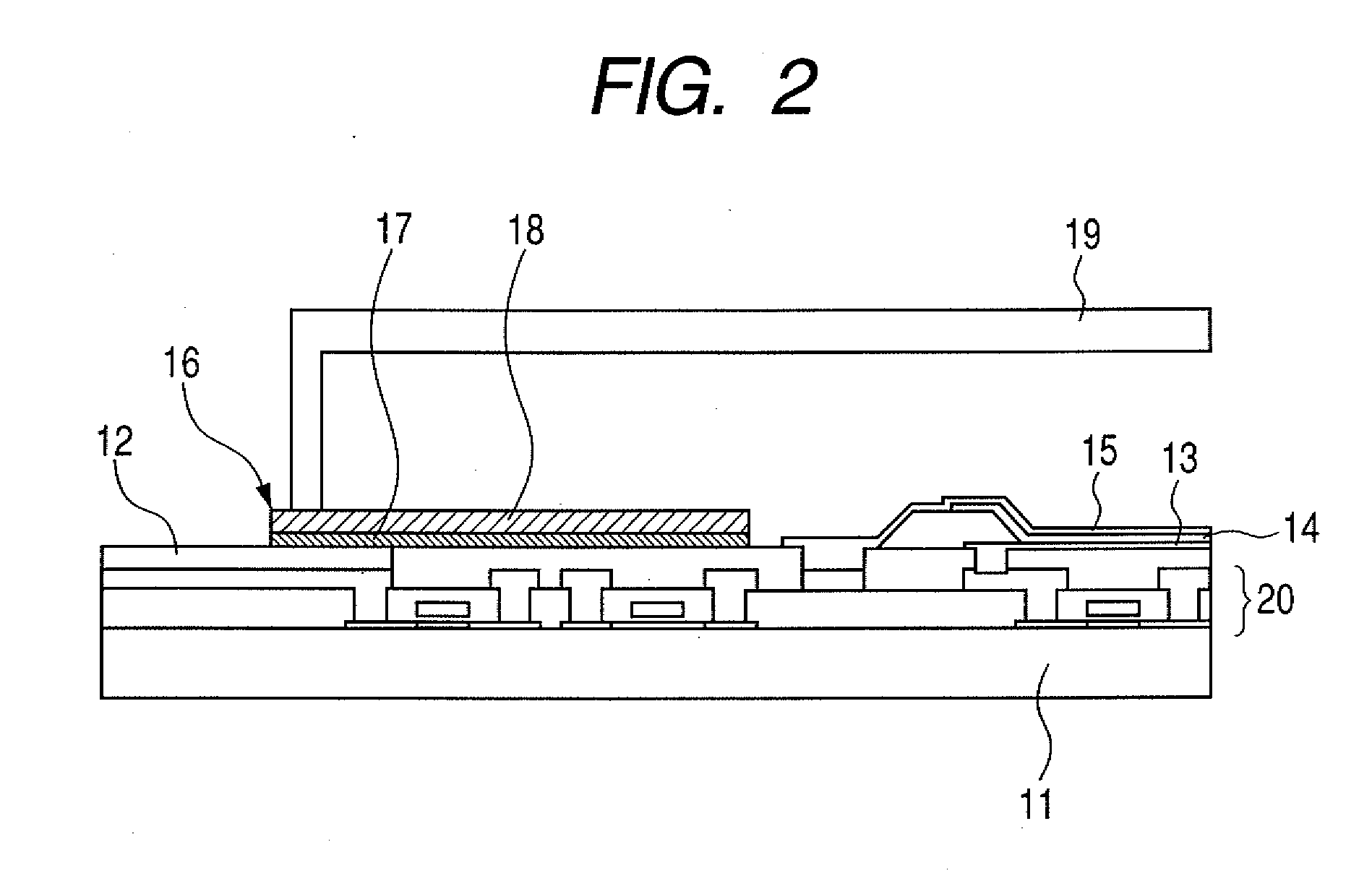
[0030]The organic EL device panel illustrated in FIG. 2 is an active drive type organic EL device panel. FIG. 2 is a partially enlarged sectional view of the organic EL device panel. In FIG. 2, the organic EL device panel includes a glass substrate 11 on which a TFT circuit 20 is formed, a lead-out wiring 12, a first electrode 13, an organic light emitting layer 14, an ITO film (second electrode) 15, a heat dissipation member 16, an insulating layer 17, a metal film 18, and a sealing glass 19. A configuration of a contact resistance portion between the lead-out wiring 12 and the power source wiring is similar to that illustr...

example 2

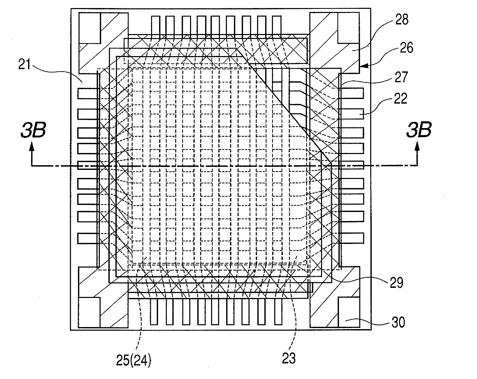
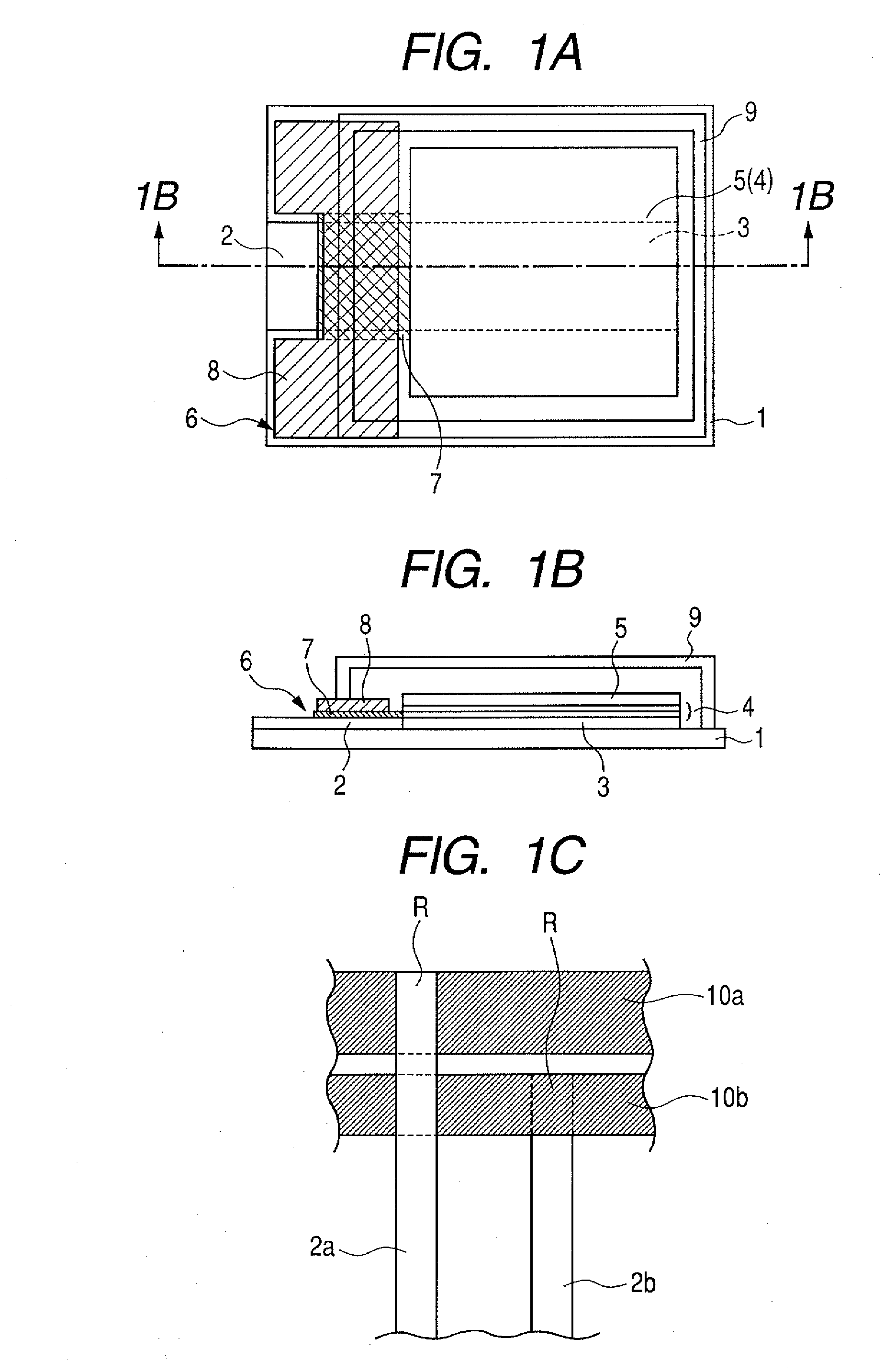
[0051]Another example of the organic EL device panel according to the present invention will be described in accordance with the manufacturing steps. The organic EL device panel illustrated in FIGS. 3A and 3B is a passive drive type organic EL device panel. FIG. 3A is a plan view schematically illustrating the organic EL device panel. FIG. 3B is a partial sectional view taken along the line 3B-3B of FIG. 3A. In FIGS. 3A and 3B, the organic EL device panel includes a grass substrate 21, a lead-out wiring 22, a first electrode 23, an organic light emitting layer 24, an ITO film (second electrode) 25, a heat dissipation member 26, an insulating layer 27, a metal film 28, a sealing glass 29, and a metal piece 30. It should be noted that the manufacturing steps of the organic EL device panel according to this example is similar to those of Example 1 except that a shape and film thickness of a mask are slightly different through steps of formation of the lead-out wiring 22 to formation of...


PUM


Abstract

There is provided an organic electroluminescence (EL) device panel including a heat dissipation member formed on a lead-out wiring electrically connected to a first electrode or a second electrode. According to the organic EL device panel of the present invention, the organic EL device is not adversely affected by heat at a time of manufacturing and driving, so deterioration of pixels of the organic EL device is not generated.

Description

BACKGROUND OF THE INVENTION[0001]1. Field of the Invention[0002]The present invention relates to an organic electroluminescence (hereinafter, abbreviated to “EL”) device panel.[0003]2. Description of the Related Art[0004]In recent years, an organic EL device which functions as a self-luminous device has been attracting attention for use in a flat panel display. The organic EL device generally has a sandwich structure in which an organic light emitting layer is sandwiched between two electrodes on a glass substrate. To allow light emitted from the organic light emitting layer to be extracted to an outside of the device, a transparent electrode is used as one of the electrodes, generally, an indium tin oxide (ITO) transparent electrode is used as an anode. Further, while an outer circumferential surface of the organic EL device is sealed with a sealing material, a current is caused to flow therein by an external driving circuit to thereby emit light.[0005]The organic EL device that em...

Claims


Application Information

Patent Timeline
Patent Type & Authority Applications(United States)
IPC IPC(8): H05B33/04H01L51/50
CPCH01L51/529H10K50/87
Inventor KANEKO, KUMIKO
Owner CANON KK
Why Eureka
Try Eureka