Panel combining method of liquid crystal display device

A technology of a liquid crystal display device and a combination method, which is applied in the fields of nonlinear optics, instruments, optics, etc., can solve the problems of cost loss of panel manufacturers and affect the display effect of the panel, and achieve the effect of weakening the mura phenomenon and dispersing the bonding pressure

Inactive Publication Date: 2007-04-18
AU OPTRONICS CORP
View PDF0 Cites 13 Cited by
  • Summary
  • Abstract
  • Description
  • Claims
  • Application Information

AI Technical Summary

Problems solved by technology

Please refer to the schematic diagram in Figure 3. After the panel 70 is assembled, there will be water ripples 60 in the display area, which will affect the ...

Method used


Image

  • Panel combining method of liquid crystal display device
  • Panel combining method of liquid crystal display device
  • Panel combining method of liquid crystal display device

Examples


Embodiment 1

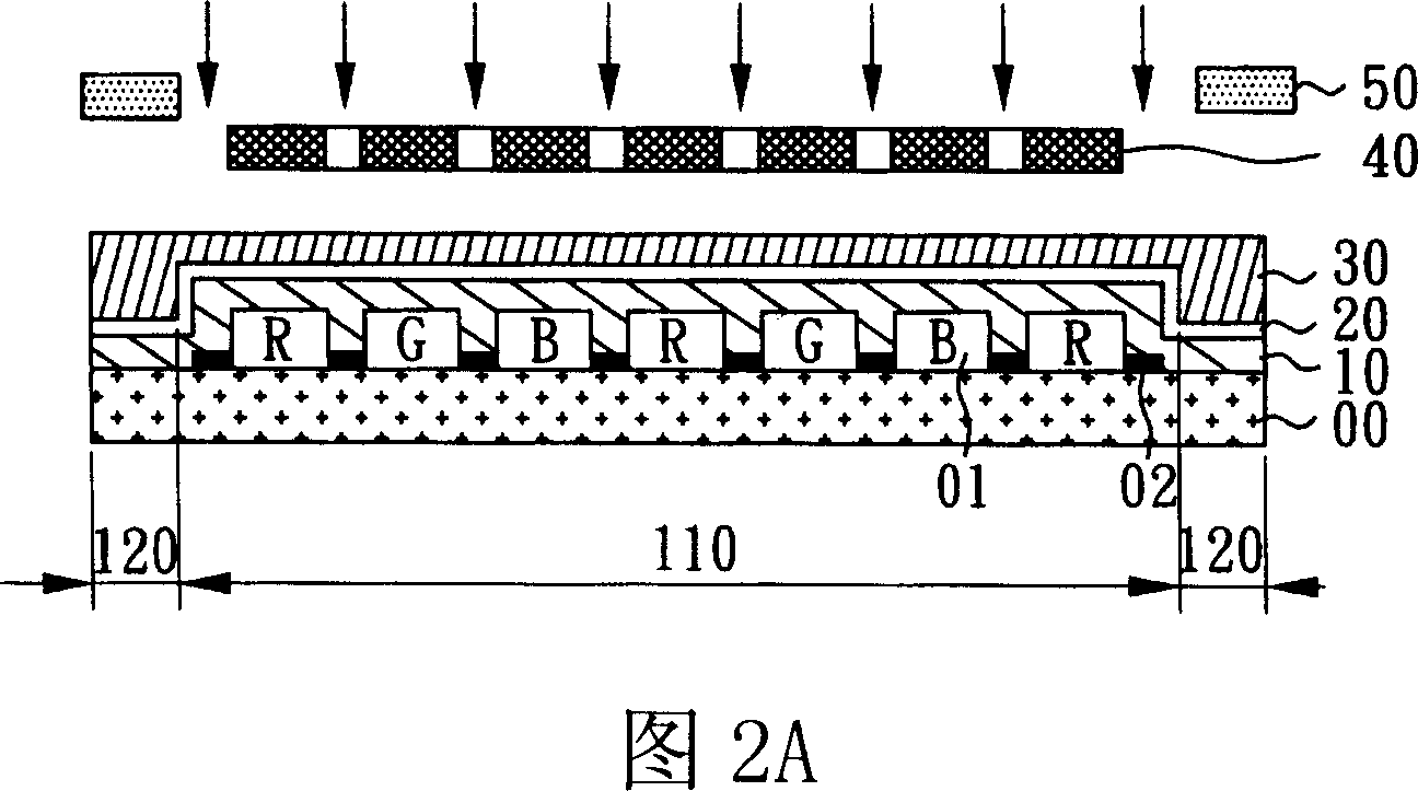
[0045] Please refer to FIG. 4 , FIG. 5A and FIG. 5B at the same time. In this embodiment, the process of fabricating photoresist-type spacers on the color filter film substrate is taken as an example to illustrate the technical features of the present invention.

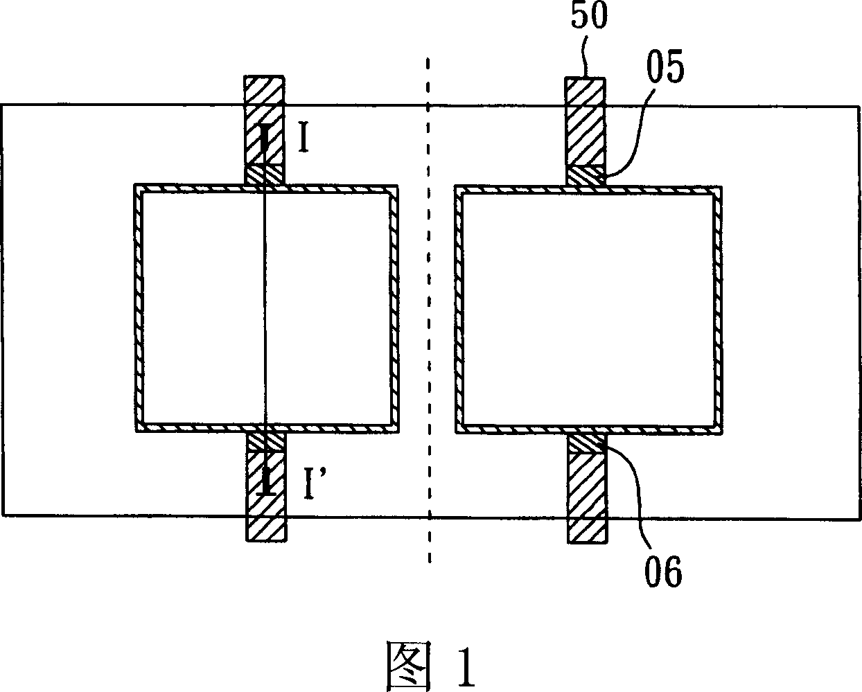
[0046] First define the size of the required color filter film on a glass substrate 00, as shown in Figure 4, the dotted line on one of the large substrates 00 is to schematically separate the areas of two color filter films 100, 200, in A display area 110 and a non-display area 120 are further defined on a single color filter film 100, and a contact area 130 of a sealant is left at the boundary between the display area 100 and the non-display area 120, so as to facilitate contact with a TFT in the subsequent process. Adhesive bonding of substrates.

[0047] Please refer to FIGS. 5A and 5B for the cross-sectional view of the line segment I to I' in the region of the color filter film 100. In FIGS.

[0048] Please refe...

Embodiment 2

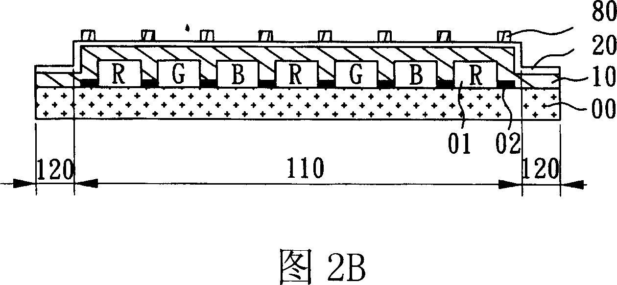
[0053] In addition to the method described in Embodiment 1, in which the spacer 90 is formed in the non-display region 120 on the CF substrate 00, this embodiment also uses FIG. 7 to illustrate another situation, which can also achieve the purpose of not causing mura in the forbidden region.

[0054] As shown in FIG. 7, a spacer 91 is formed on the outer edge of the original exposure forbidden area 05. The steps for forming the spacer 91 are roughly the same as those described in Embodiment 1, except that the mask patterns used are different. In this example a U-shaped washer is shown, and the mask used will suffice with the corresponding pattern.

[0055] In the above-mentioned embodiment, when the negative photoresist is used for exposure and development, the cover plate that originally covered the gap in the forbidden area is removed, and a large area is directly formed in the forbidden area where no photoresist-type spacers were originally formed. At the same time, other p...


PUM


Abstract

The invention relates to liquid crystal display device panel combination method. It includes the following steps: preparing one color light filter base plate includes one display area and one non display area of which edge location are set at lease two interval cushion of which height is the same as the photo-resist type interval end in the display area, and thin film transistor array base plate; binding the two base plates. The produced base plate can avoid color uneven for panel exclusion area to increase base plate technology qualified rate.

Description

technical field [0001] The invention relates to a panel assembly method of a liquid crystal display device, in particular to a panel assembly method for improving the phenomenon of color unevenness (mura) on the forbidden area of ​​the panel. Background technique [0002] The manufacturing process of thin film transistor liquid crystal display (TFT LCD) panels can be divided into three parts: upstream substrate manufacturing, midstream panel assembly (Cell), and downstream module assembly (Module). Among them, upstream substrate manufacturing and midstream panel assembly are the front-end manufacturing process of panel manufacturing, while downstream module assembly uses the completed panel to install the backlight module and driver circuit board to complete the assembly of the LCD module. Among them, the manufacture of the substrate can be further divided into two parts: the manufacture of the thin film transistor array substrate (TFT substrate) and the manufacture of the c...

Claims


Application Information

Patent Timeline
IPC IPC(8): G02F1/1339G02F1/1333G02F1/1335
Inventor 詹嘉豪李如玉林锦松林传杰
Owner AU OPTRONICS CORP
Why Eureka
Try Eureka