Substrate bonding apparatus for liquid crystal display device panel
- Summary
- Abstract
- Description
- Claims
- Application Information
AI Technical Summary
Benefits of technology
Problems solved by technology
Method used
Image
Examples
Embodiment Construction
[0026] Reference will now be made in detail to the preferred embodiments of the present invention, examples of which are illustrated in the accompanying drawings.
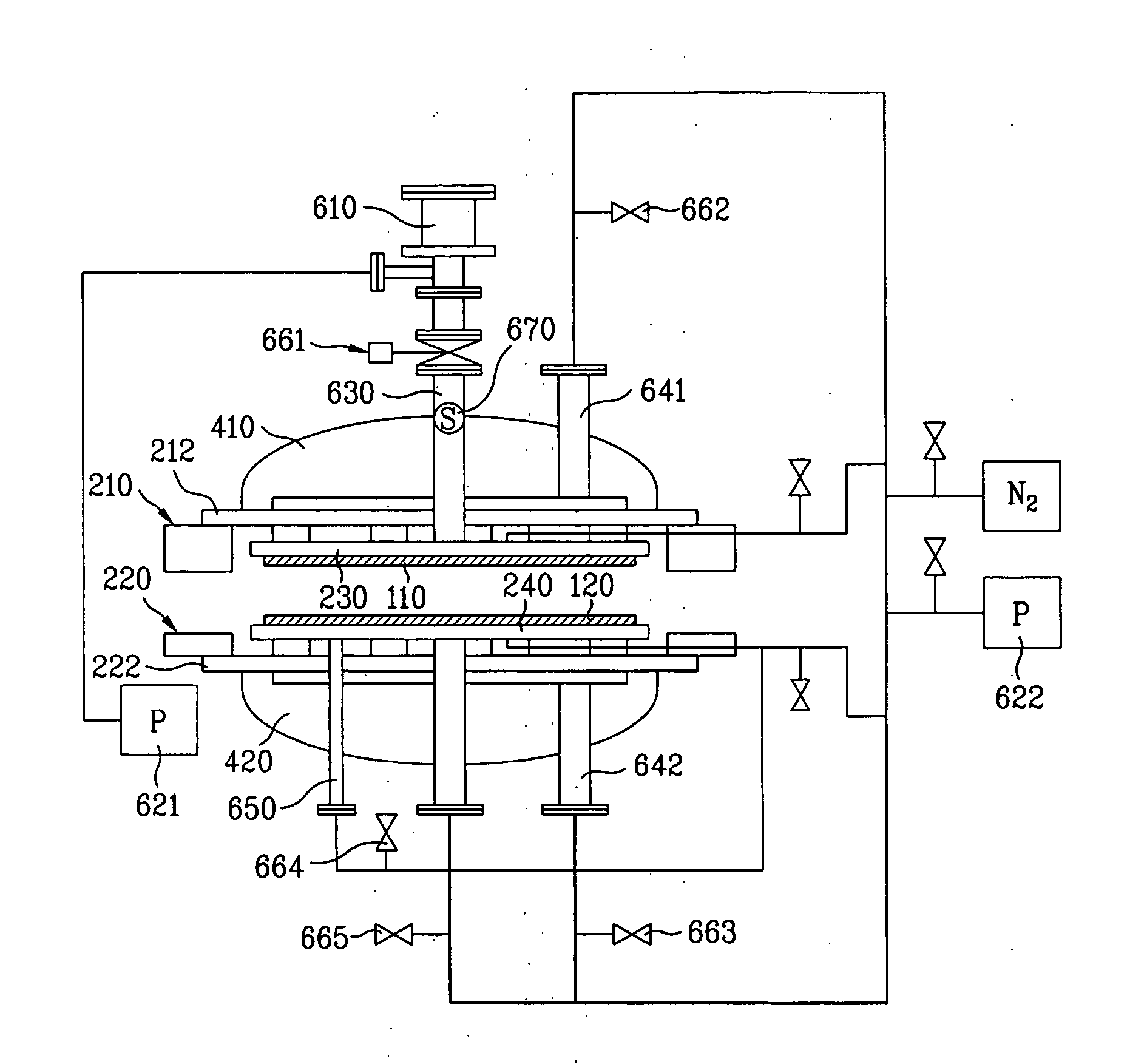
[0027]FIG. 3 is a cross sectional view of an exemplary substrate bonding apparatus for fabricating an LCD panel according to the present invention. In FIG. 3, a substrate bonding apparatus may include a base frame 100, an upper chamber unit 210, a lower chamber unit 220, an upper stage 230, and a lower stage 240. The substrate bonding apparatus may also include an interlocking system 510 and a support system 710. In addition, although not specifically shown, the substrate bonding apparatus may include a chamber moving system, a sealing system, alignment cameras, an alignment system, a vacuum pumping system, and high and low vacuum chambers.
[0028] The base frame 100 may be fixed to a floor structure (not shown), and may form an exterior of the substrate bonding apparatus. In addition, the base frame 100 may simultaneously ...
PUM
| Property | Measurement | Unit |
|---|---|---|
| Force | aaaaa | aaaaa |
| Vacuum | aaaaa | aaaaa |
| Electrostatic force | aaaaa | aaaaa |
Abstract
Description
Claims
Application Information


