Directed assembly of highly-organized carbon nanotube architectures

a carbon nanotube and architecture technology, applied in the field of carbon nanotubes, can solve the problems of reducing the efficiency of carbon nanotubes, so as to achieve the effect of reducing the difficulty of obtaining nanotubes that are exclusively oriented parallel to the substrate in predetermined orientations

Inactive Publication Date: 2007-09-20
RENESSELAER POLYTECHNIC INST
View PDF16 Cites 95 Cited by
  • Summary
  • Abstract
  • Description
  • Claims
  • Application Information

AI Technical Summary

Problems solved by technology

However, the present techniques used to controllably build organized architectures of nanotubes with predetermined orientations have several deficiencies.
However, this technique requires deposition and patterning, usually in separate processing steps, of catalyst material, typically in nanoparticle assemblies or thin film forms, which complicates the nanotube fabrication method.
This also does not allow growth of nanotubes in more than one preselected orientation at different locations in a controllable fashion.
While growth of vertically aligned nanotubes on planar substrates by CVD has been reported extensively, obtaining nanotubes that are exclusively oriented parallel to the substrate in predetermined orientations has been more difficult.
However, these approaches require pre-deposition and pre-patterning of nanoscale catalyst particle assemblies.
Also, the probability of nanotubes bridging across different catalyst islands is difficult to predict and control.
However, these methods are also complicated, and are difficult to scale (e.g., create them reproducibly on an 8 inch Si wafer) and to control, for developing devices for applications.
Moreover, in these cases the nanotubes are not rooted to the substrate (i.e. they are just lying on them, and hence not very robust).
However, as can be seen in FIG. 4 of the Z. J. Zhang et al. article, while roughly vertical and horizontal nanotubes were simultaneously grown on the template structures, it was not possible to controllably align nanotubes during growth in a direction perpendicular to the silica template structure surfaces.

Method used


Image

  • Directed assembly of highly-organized carbon nanotube architectures
  • Directed assembly of highly-organized carbon nanotube architectures
  • Directed assembly of highly-organized carbon nanotube architectures

Examples


first embodiment

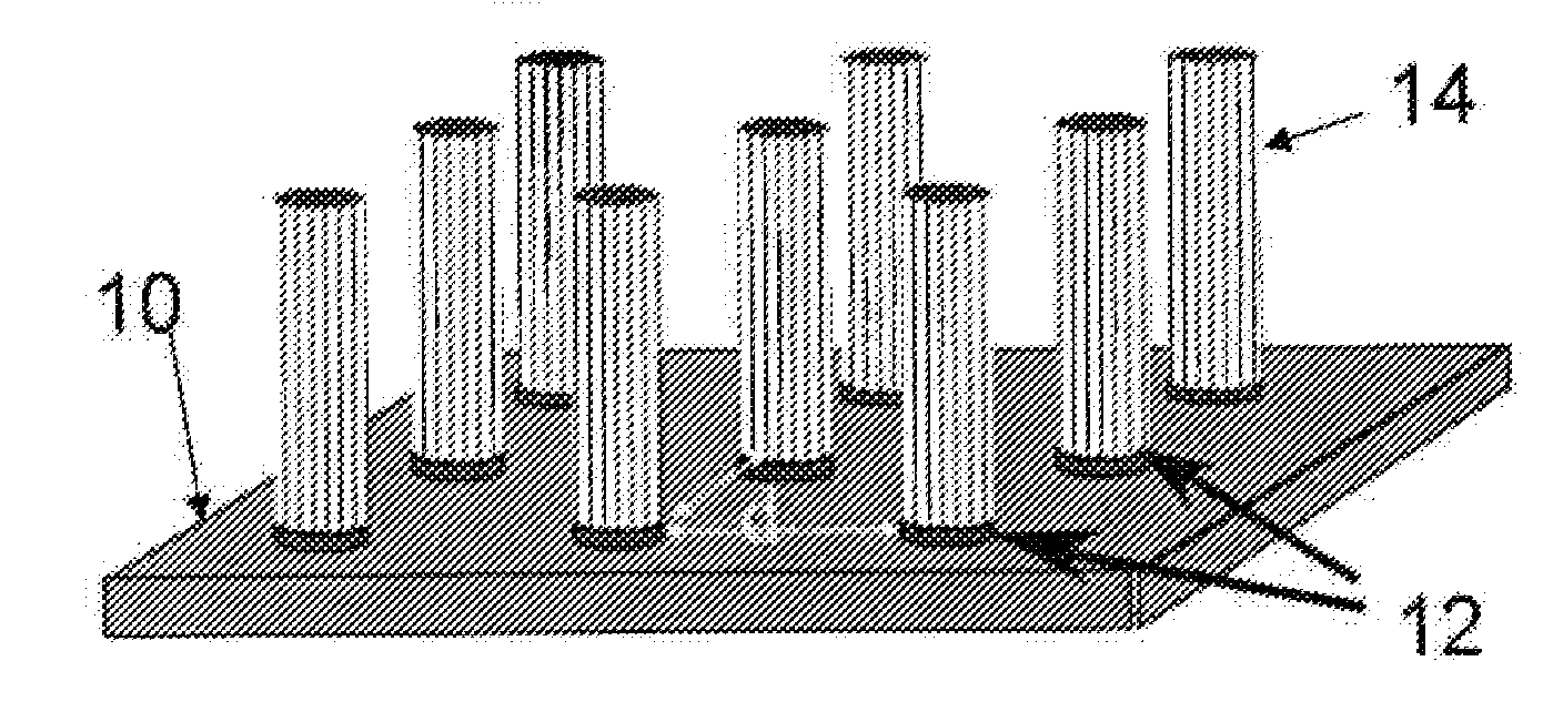
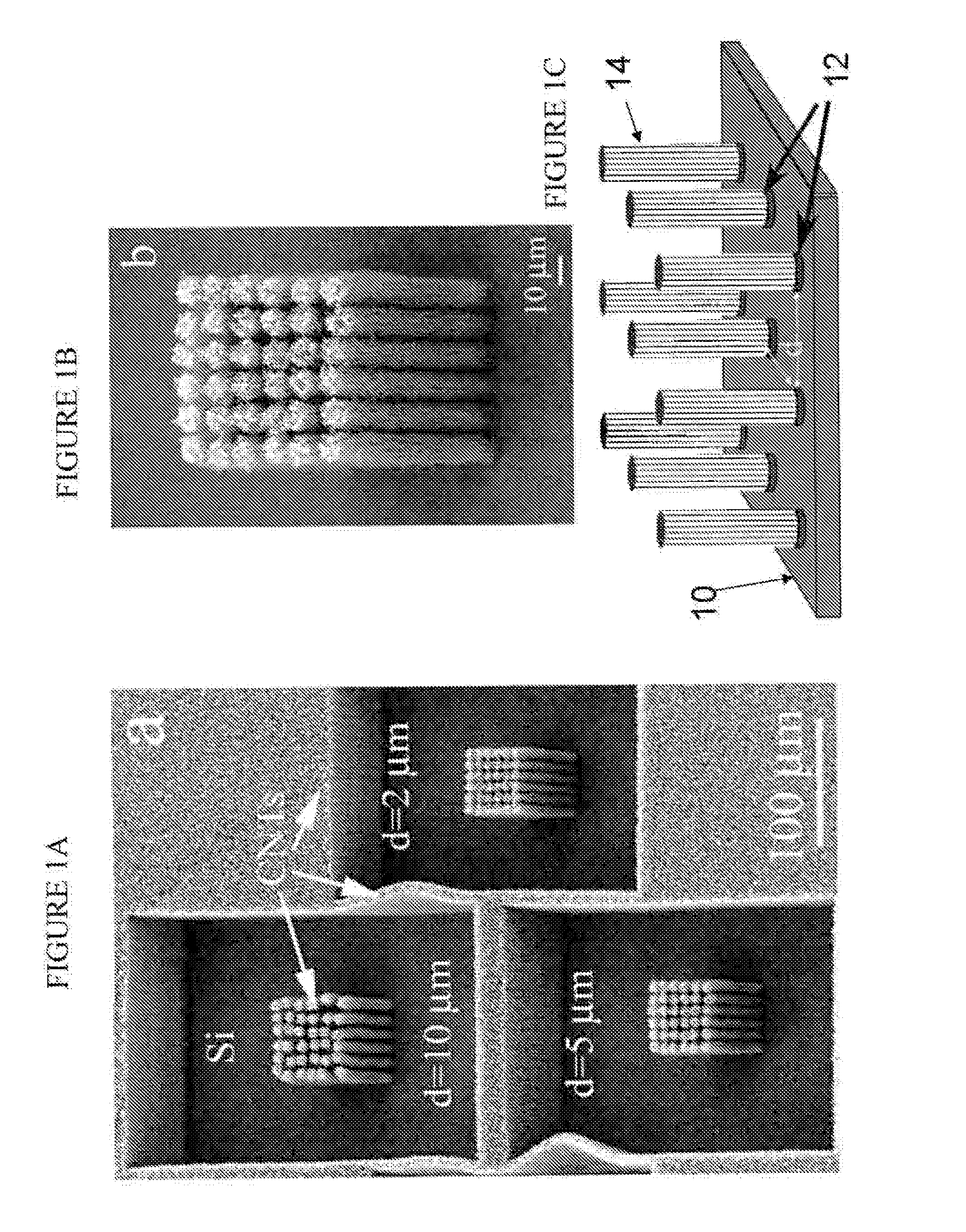
[0029] FIGS. 1A-B show a striking example of aligned nanotube pillars placed on specific sites on the substrate according to one aspect of the FIG. 1A illustrates an SEM image of pillars of aligned carbon nanotube (CNT) arrays within trenches surrounded by a thick aligned nanotube film grown vertically on the SiO2 pattern on a Si substrate. The nanotube film was selectively grown on a SiO2 pattern or template structure. In the center of box-like regions defined by the nanotube film walls, micro-sized cylindrical blocks or pillars of vertically oriented nanotubes are grown from the underlying template structure constituted by SiO2 patterns in this case. Within each block, the nanotubes are highly oriented and densely packed. Three different pillar packing densities are shown in FIG. 1A, where the separation between pillars in each group is 10 microns (top), 5 microns (bottom) and 2 microns (center).

[0030]FIG. 1B is an enlarged image of the middle array shown in FIG. 1A showing the a...

second embodiment

[0037] The porous nanotube films were obtained by using a porous template structure or layer formed over a substrate. For example, a porous silica template layer was obtained by forming a silica layer on the silicon substrate and then photolithographically masking the layer and etching pores or holes in this layer. Since the pores or holes are formed by photolithography and etching, they have a controlled size. The pores or holes extend down to the silicon substrate and may extend into the silicon substrate if desired. Thus, portions of the substrate are exposed through pores in the porous template layer. Nanotube-forming gases or mixtures were provided onto the porous template layer and the carbon nanotubes were selectively grown on the porous template layer. However, the nanotubes were not formed on portions of the substrate exposed through pores in the porous template layer. Furthermore, the nanotubes did not form on the template layer pore sidewalls because the template layer th...

third embodiment

[0039] The method and structure of the third preferred embodiment will now be described. In the third embodiment, selective nanotube growth on the template structure having at least one, and preferably two or more surfaces. The nanotube growth occurs in a direction normal to the respective surfaces and hence this approach can be harnessed to simultaneously grow nanotubes in several predetermined directions. For example, nanotube growth in mutually orthogonal directions may be carried out by using template structures comprising of deep etched trenches, drilled all the way to silicon substrate, separating several thick SiO2 template structure towers. Preferably, the nanotubes are grown on side surfaces of the template structures, which are preferably thicker than about 200 nm, preferably thicker than 2 microns. For example, the template structure may be several microns thick, such as 2 to 10 microns thick, preferably 5 to 8.5 microns thick. However, thickness of the template structure...


PUM

PropertyMeasurementUnit
temperatureaaaaaaaaaa
diameteraaaaaaaaaa
diameteraaaaaaaaaa

Abstract

A method of controllably aligning carbon nanotubes to a template structure to fabricate a variety of carbon nanotube containing structures and devices having desired characteristics is provided. The method allows simultaneous, selective growth of both vertically and horizontally controllably aligned nanotubes on the template structure but not on a substrate in a single process step.

Description

CROSS-REFERENCE TO RELATED PATENT APPLICATIONS [0001] The present application is a Divisional of U.S. application Ser. No. 10 / 361,640, filed Feb. 11, 2003, which claims benefit under 35 U.S.C. § 119(e) of U.S. provisional application 60 / 356,069, filed Feb. 11, 2002 and 60 / 385,393, filed Jun. 3, 2002, both of which are incorporated herein by reference in their entirety.STATEMENT REGARDING FEDERALLY SPONSORED RESEARCH OR DEVELOPMENT [0002] The U.S. Government may have certain rights in this invention pursuant to grant number N00014-00-1-2050 from the Office of Naval Research.BACKGROUND OF THE INVENTION [0003] The present invention relates generally to carbon nanotubes and more particularly to selective growth of carbon nanotubes on template materials. [0004] It is likely that future devices containing organized structures of various functional materials with new properties will be built from nanoscale building blocks. These nanoscale building blocks can be produced by a variety of syn...

Claims


Application Information

Patent Timeline
Patent Type & Authority Applications(United States)
IPC IPC(8): C23C16/00B82B1/00B82B3/00C01B31/02C04B35/14C30B33/00H01M4/58H01M4/583
CPCB82Y30/00Y10T428/139C01B31/0226C01B2202/08C04B35/14C04B35/62802C04B35/62839C04B2235/3206C04B2235/3217C04B2235/3418C04B2235/5264C04B2235/528C04B2235/5288C30B33/00H01M4/583B82Y40/00C30B29/605C01B32/16Y02E60/10
Inventor AJAYAN, PULICKEL M.RAMANATH, G.WEI, BINGQINGCAO, ANYUANJUNG, YUNG JOON
Owner RENESSELAER POLYTECHNIC INST
Why Eureka
Try Eureka