Light-emitting diode and method for manufacturing the same

Inactive Publication Date: 2007-09-27
EPISTAR CORP
View PDF2 Cites 17 Cited by
  • Summary
  • Abstract
  • Description
  • Claims
  • Application Information

AI Technical Summary

Benefits of technology

[0015]The anodic oxidation metal layer including nano holes orderly distributed in the light-extracting surface of the light-emitting diode can be formed to easily achieve the effect of roughening the light-extracting surface of the light-emitting diode by performing an anodic oxidization step and an et

Problems solved by technology

However, in this conventional method for roughening the surface, the uniformity of the roughening surface is poor.
However, the processes of the second method and the third metho

Method used


Image

  • Light-emitting diode and method for manufacturing the same
  • Light-emitting diode and method for manufacturing the same
  • Light-emitting diode and method for manufacturing the same

Examples


Embodiment Construction

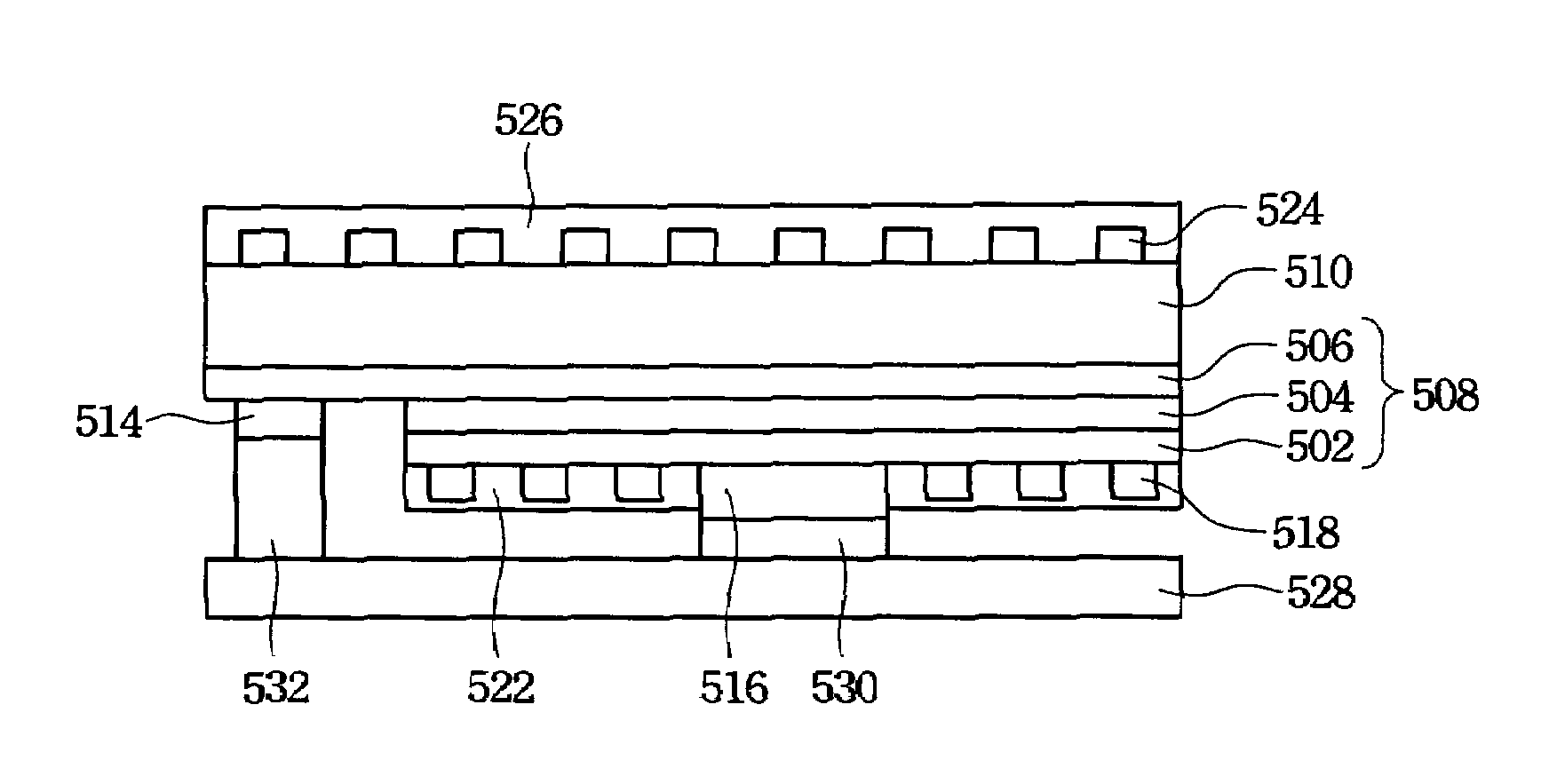
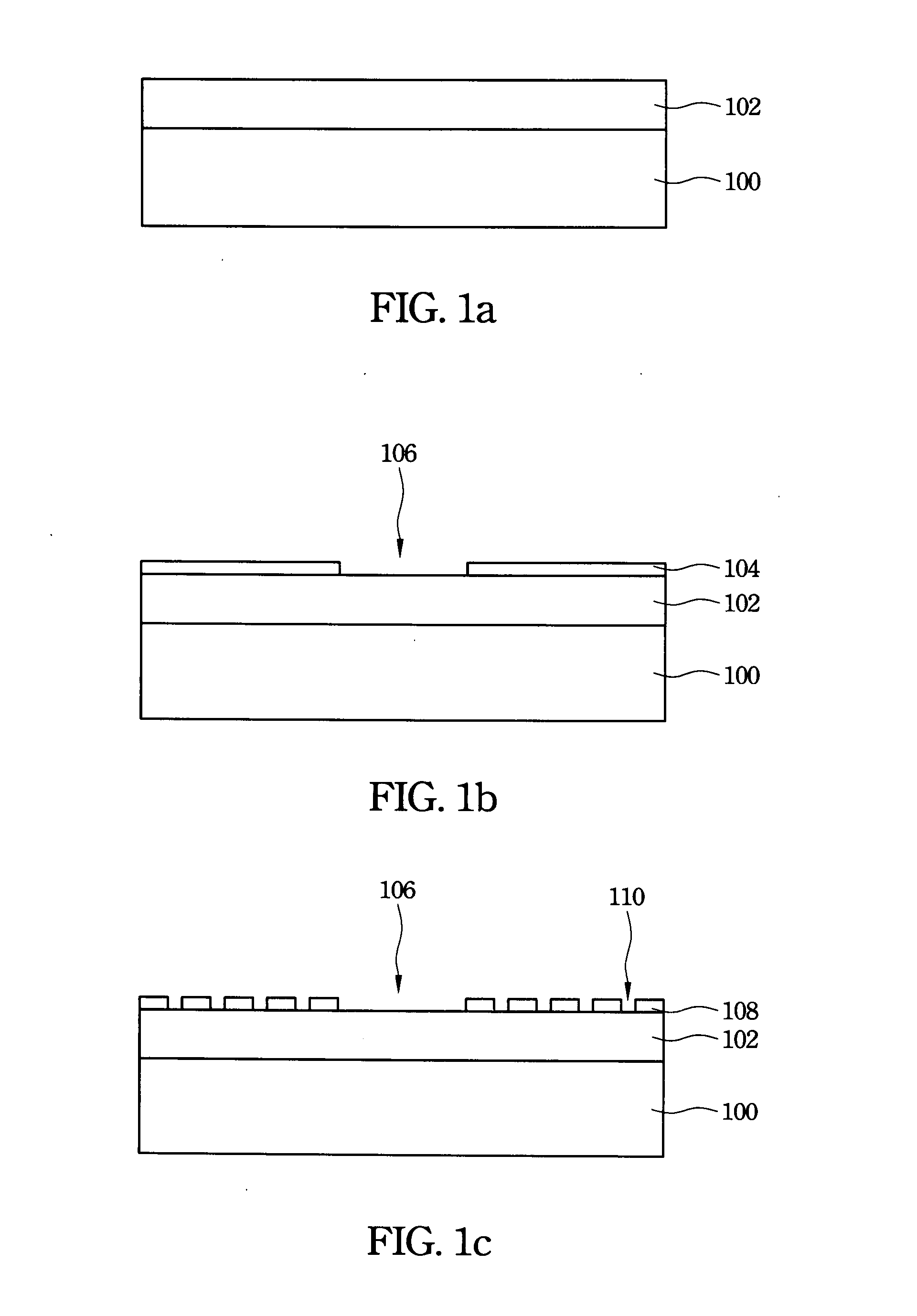
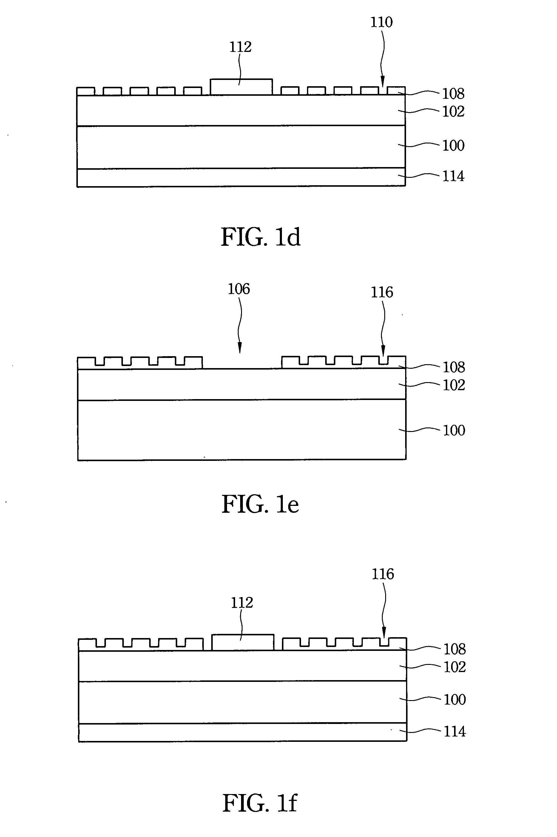
[0026]The present invention discloses a light-emitting diode and a method for manufacturing the same, in which the effect of uniformly roughening the light-emitting surface of the light-emitting diode device can be easily achieved by an anodic oxidization and etching method. In order to make the illustration of the present invention more explicit, the following description is stated with reference to FIGS. 1a through 5f.

[0027]FIGS. 1a through 1d are schematic flow diagrams showing the process for manufacturing a light-emitting diode in accordance with a first preferred embodiment of the present invention. Firstly, a substrate 100 is provided, wherein the substrate 100 includes two opposite surfaces. The substrate 100 may be made of a semiconductor material, such as GaAs or InP. An illuminant epitaxial structure 102 is grown on a surface of the substrate 100 by, for example, an epitaxial method, as shown in FIG. 1a. The illuminant epitaxial structure 102 is composed of AlGaInP based...


PUM


Abstract

A light-emitting diode (LED) and a method for manufacturing the same are described. The method for manufacturing the LED comprises the following steps. An illuminant epitaxial structure is provided, in which the illuminant epitaxial structure has a first surface and a second surface on opposite sides, and a substrate is deposed on the first surface of the illuminant epitaxial structure. A metal layer is formed on the second surface of the illuminant epitaxial structure. An anodic oxidization step is performed to oxidize the metal layer, so as to form a metal oxide layer. An etching step is performed to remove a portion of the metal oxide layer, so as to form a plurality of holes in the metal oxide layer.

Description

RELATED APPLICATIONS[0001]The present application is based on, and claims priority from, Taiwan Application Serial Number 95109340, filed Mar. 17, 2006, the disclosure of which is hereby incorporated by reference herein in its entirety.FIELD OF THE INVENTION[0002]The present invention relates to a method for manufacturing a light-emitting diode (LED), and more particularly, to a method for increasing the light extraction efficiency of a light-emitting diode.BACKGROUND OF THE INVENTION[0003]Semiconductor light-emitting devices, such as light emitting diodes (LED), are formed by using semiconductor materials. The semiconductor light emitting devices are one kind of minute solid-state light sources that can transform electrical energy into light energy. The semiconductor light emitting devices are not only small in volume, use a low driving voltage, rapid in response speed, shockproof, and long-lived, but also can meet the lightness, thinness, and miniaturization needs of various appar...

Claims


Application Information

Patent Timeline
IPC IPC(8): H01L33/00H01L21/00H01L33/12H01L33/32H01L33/42H01L33/62
CPCH01L33/22H01L2933/0091H01L33/44
Inventor CHEN, SHI-MINGHOUNG, MAU-PHONCHU, CHANG-HSINGYEN, TE-CHI
Owner EPISTAR CORP
Why Eureka
Try Eureka