

Printed Circuit Board and Manufacturing Method Thereof
a technology of printed circuit boards and manufacturing methods, applied in the direction of high-frequency circuit adaptations, coupling device connections, transportation and packaging, etc., can solve the problems of degrading the transmission efficiency of electrical signals, and achieve the effect of reducing the variability of characteristic impedances, ensuring the transmission efficiency of electrical signals, and sufficient flexibility
Inactive Publication Date: 2007-10-04
NITTO DENKO CORP
View PDF10 Cites 6 Cited by
- Summary
- Abstract
- Description
- Claims
- Application Information
AI Technical Summary
Benefits of technology
[0020]It is an object of the invention to provide a printed circuit board in which sufficient flexibility can be sec
Problems solved by technology
If they do not match, a part of the electrical signal is reflected at the connection part between the wirin
Method used
View moreImage
Smart ImageViewing Examples

Examples
 PUM
| Property | Measurement | Unit |
|---|---|---|
| Thickness | aaaaa | aaaaa |
| Thickness | aaaaa | aaaaa |
| Electrical conductor | aaaaa | aaaaa |
Abstract
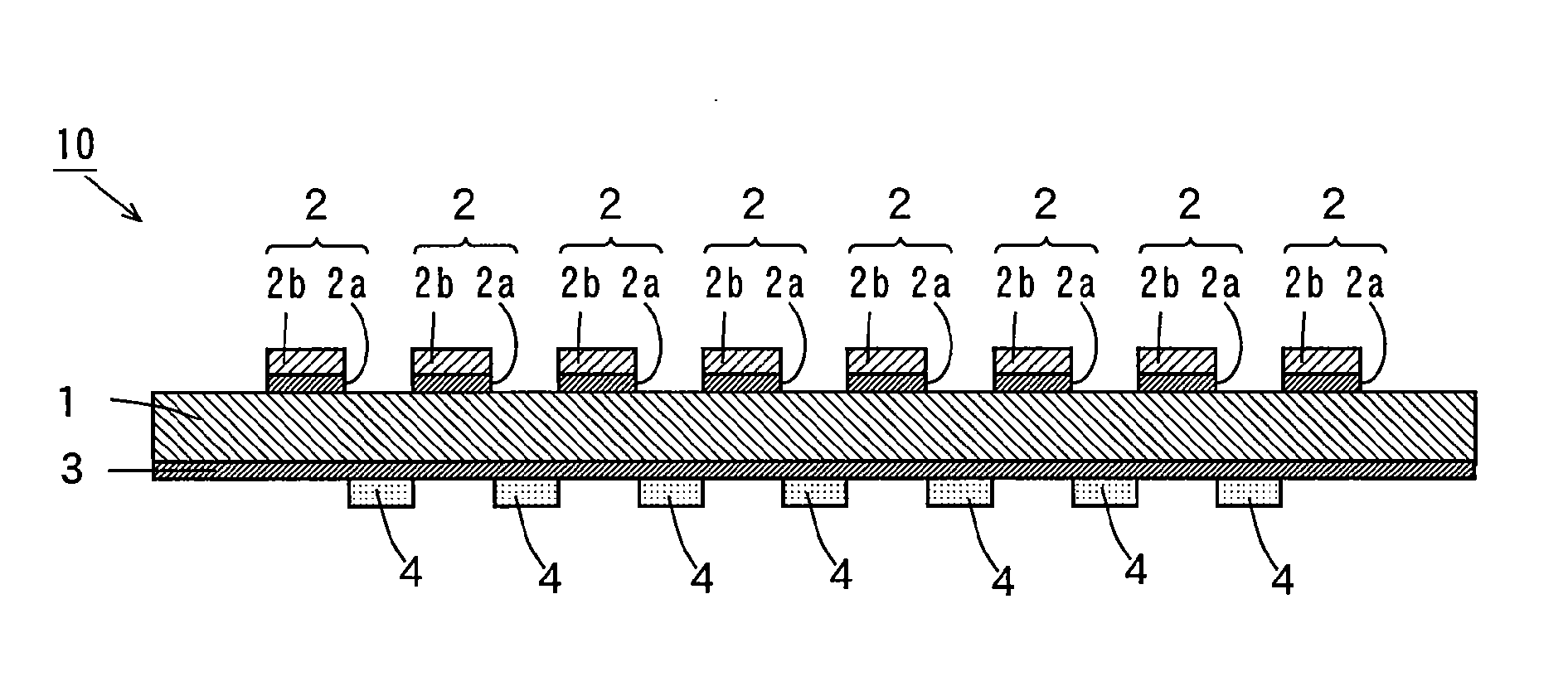
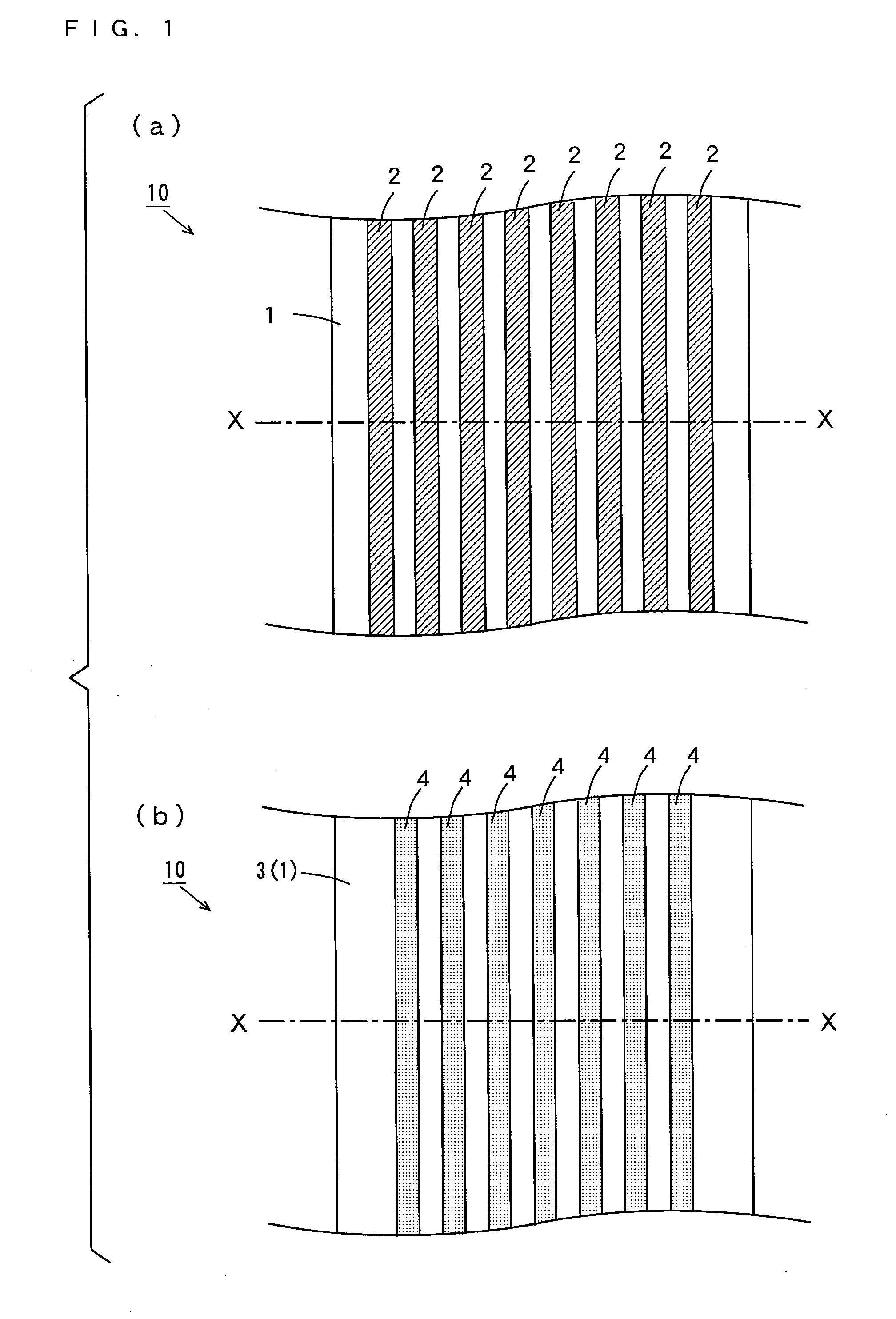
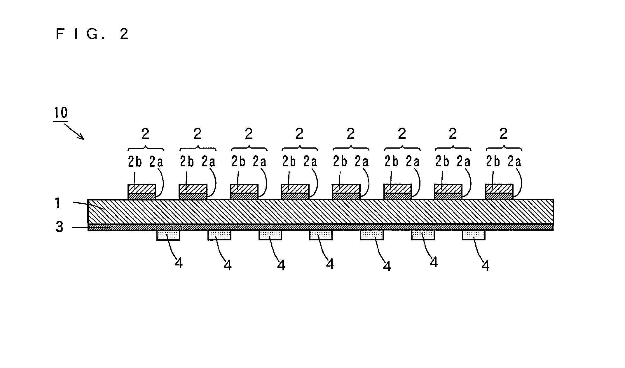
A plurality of wiring patterns in a stripe form are formed to be parallel to one another on one surface of a base insulating layer. The wiring patterns each have a layered structure including a conductive layer and a wiring layer. A thin metal film is formed on the other surface of the base insulating layer, and a plurality of ground patterns in a stripe form are formed to be parallel to one another on the thin metal film. The wiring patterns and the ground patterns are provided in a staggered manner so that they are not opposed to one another with the base insulating layer interposed therebetween. In other words, the ground patterns are provided to be opposed to regions between the wiring patterns.
Description
BACKGROUND OF THE INVENTION[0001]1. Field of the Invention[0002]The present invention relates to a printed circuit board and a manufacturing method thereof.[0003]2. Description of the Background Art[0004]A flexible printed circuit board that can be bent is used for a movable element in electronic equipment. The flexible printed circuit board for example has wiring patterns made of a conductor formed on one surface of an insulating layer and a ground layer formed on the other surface. The wiring patterns are connected to various kinds of electronic components and transmit electrical signals between these electronic components.[0005]In the flexible printed circuit board, various techniques have been devised in the ground layer to secure necessary flexibility.[0006]FIG. 8 shows an example of a conventional flexible printed circuit board (see JP 2004-088020A). Hereinafter, the flexible printed circuit board will be abbreviated as “printed circuit board.”[0007]FIG. 8(a) is a plan view of...
Claims
Login to View More Application Information
Patent Timeline
 IPC IPC(8): H05K1/03
CPCH05K1/0224H05K1/0253H05K3/108H05K2201/0373Y10T428/24926H05K2201/09709H05K2201/09736Y10T428/24917H05K2201/09236
Inventor HONJO, MITSURU
Owner NITTO DENKO CORP