Light emitting device and fabrication method thereof

a technology of light emitting device and fabrication method, which is applied in the direction of semiconductor devices, basic electric elements, electrical apparatus, etc., can solve the problems of insufficient and worse device performance, and achieve the effect of increasing the extraction efficiency of light which is emitted in the light emitting devi

Active Publication Date: 2007-10-04
NICHIA CORP
View PDF4 Cites 47 Cited by
  • Summary
  • Abstract
  • Description
  • Claims
  • Application Information

AI Technical Summary

Benefits of technology

[0043]According to the present invention, since a light which is radiated from the side of the light emitting area can be effectively reflected in the observation surface direction by forming the insulation film on the top of the protrusions and depressions to be thicker than that of other areas, extraction efficiency of a light which is emitted in a light emitting device can be increased. In addition, since the insulation film in an area other than the top of the protrusions and depressions is formed to be relatively thin, the light can be effectively extracted outside without an additional absorption of the light when the light is extracted outside through the i

Problems solved by technology

In addition, when openings are formed in the light emitting area, a device performance becomes worse due to, for example, increase in a resistance of the LED.
In the light emitting device described in the Japanese Laid-open Patent Publication No. 2004-221529, since a height of disposed protrus

Method used


Image

  • Light emitting device and fabrication method thereof
  • Light emitting device and fabrication method thereof
  • Light emitting device and fabrication method thereof

Examples


first embodiment

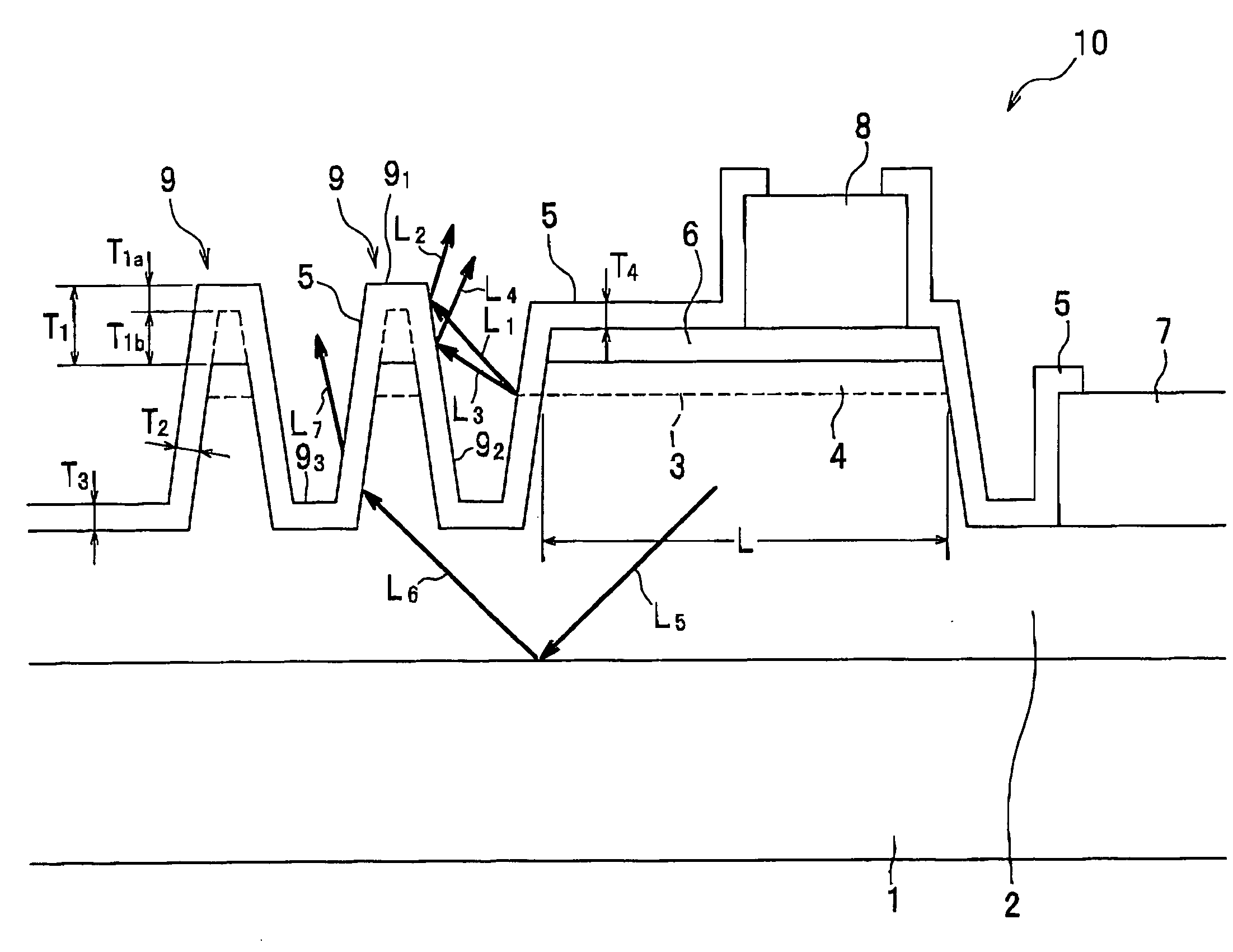
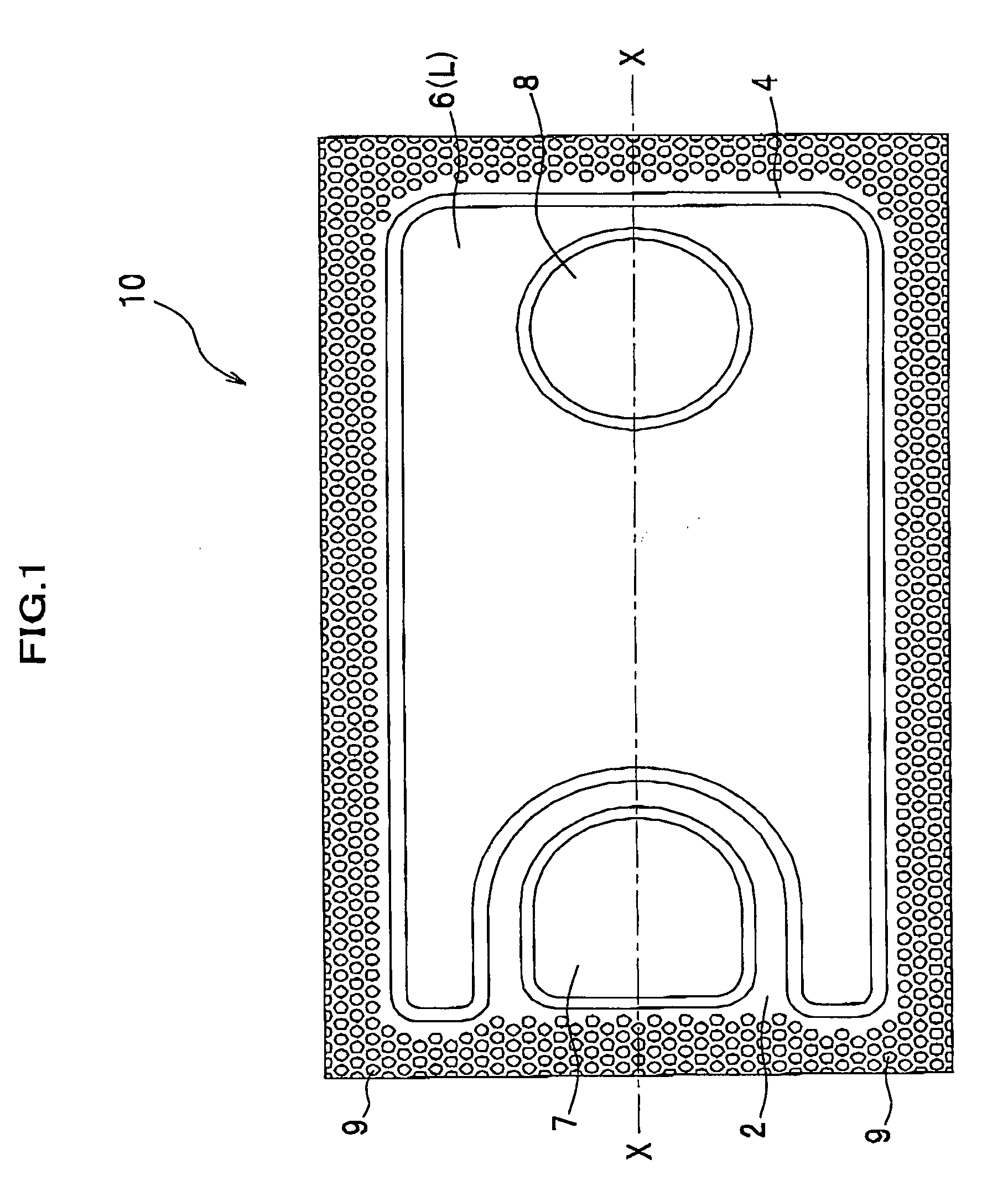
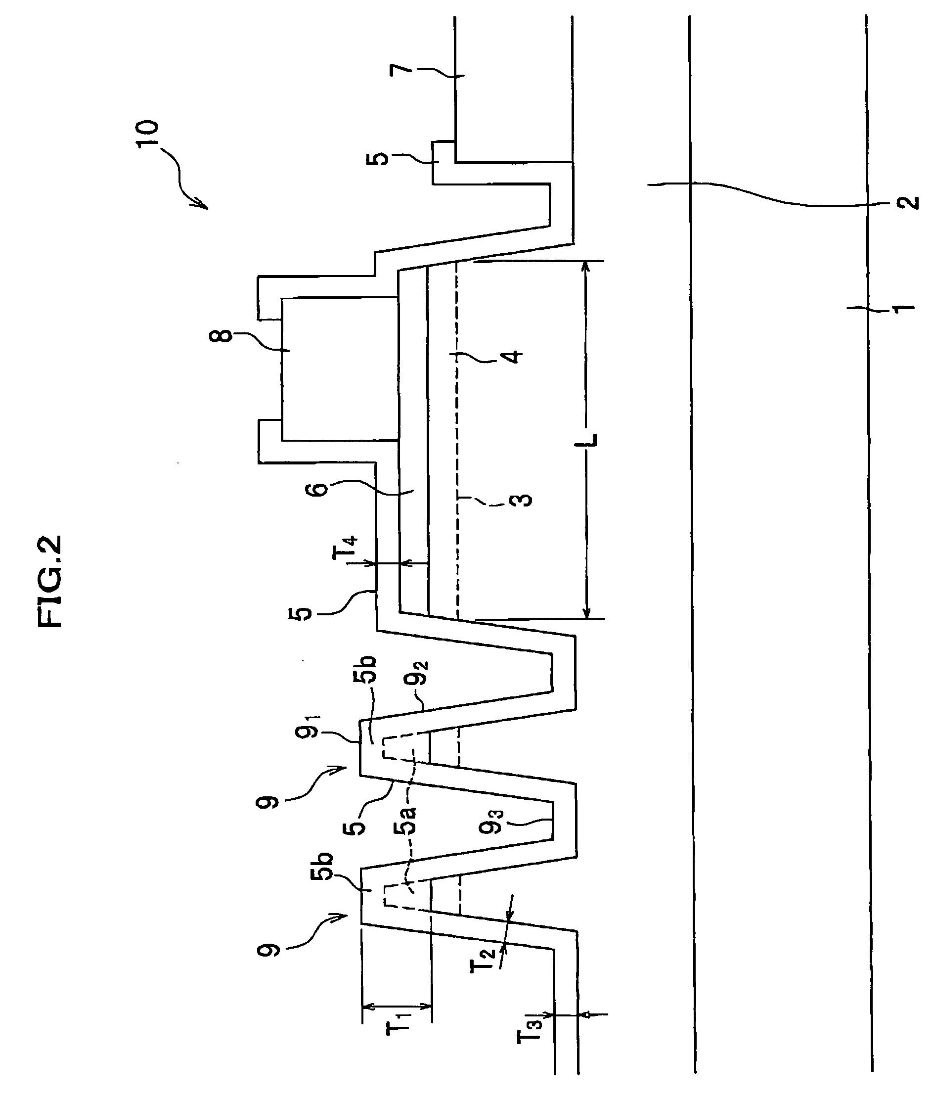
[0069]An LED 10 according to a first embodiment will be explained by referring to FIG. 1 and FIG. 2. FIG. 1 is a plane view of an LED according to the first embodiment, which is seen from an electrode arrangement side. FIG. 2 is a schematic cross sectional view which includes an n-side electrode (hereinafter, referred to as n-electrode), a p-side electrode (hereinafter, referred to as p-electrode), and the protrusions, taken along a line X-X of FIG. 1.

[0070]In the first embodiment, a semiconductor stack structure which configures an LED structure is formed on a substrate 1 made of sapphire, and the p-electrode 8 and the n-electrode 7 are arranged on a surface of a same side (surface of the substrate 1, on which semiconductor stack structure is formed, that is, upward surface in FIG. 2). A light is extracted from the electrode arrangement side on which an observation surface direction is set. The semiconductor stack structure which configures an LED 10 is formed by sequentially stack...

second embodiment

[0177]Next, the LED 10 according to a second embodiment will be explained by referring to FIG. 5. FIG. 5 is a plane view of the LED 10 according to the second embodiment, which is seen from an electrode arrangement side.

[0178]The LED 10 according to the second embodiment has an identical configuration to that of the LED 10 according to the first embodiment except disposing the protrusions 9 between the n-electrode 7 and the transparent electrode 6 which is arranged so as to surround the n-electrode 7.

[0179]The LED 10 according to the second embodiment is provided with the protrusions 9 in a single line between the n-electrode 7 and the transparent electrode 6 which is arranged so as to surround the n-electrode 7.

[0180]In the LED 10 according to the first embodiment shown in FIG. 1, a light which is radiated from the side of the light emitting area L which faces the n-electrode 7 is absorbed or diffused by the n-electrode 7, or propagates in the lateral direction, keeping the origina...

third embodiment

[0181]Next, the LED 10 according to a third embodiment will be explained by referring to FIG. 6. FIG. 6 is a plane view of the LED 10 according to the third embodiment, which is seen from an electrode arrangement side. The LED 10 according to the third embodiment has an identical configuration to that of the LED 10 according to the first embodiment except a shape of a semiconductor stack structure, a shape of the transparent electrode 6 caused by a change of the shape of the semiconductor stack structure, and an area where the protrusions 9 are arranged.

[0182]In the LED 10 according to the third embodiment, when the LED 10 is seen from the electrode arrangement side, the semiconductor stack structure which is formed in the light emitting area L located between the n-electrode 7 and the p-electrode 8 has a constricted part which becomes narrower toward the p-electrode 8 from the n-electrode 7 on a straight line X-X which connects the n-electrode 7 and the p-electrode 8, and a plurali...


PUM


Abstract

A light emitting device which includes: a substrate; an n-type semiconductor layer which is composed of a nitride semiconductor, formed on the substrate and has an n-side electrode; a p-type semiconductor layer which is composed of a nitride semiconductor, and stacked above the n-type semiconductor layer; a light emitting layer which is disposed between the n-type semiconductor layer and the p-type semiconductor layer; a p-side electrode which is disposed on a transparent electrode formed on the p-side electrode in a light emitting area; a plurality of protrusions and depressions in an area other than the light emitting area; and an insulation film on an area except areas of the n-side electrode and the p-side electrode, wherein the n-side electrode and the p-side electrode are arranged on a same side of the substrate, wherein a thickness of the insulation film on a top of the protrusions and depressions is thicker than a thickness of the insulation film in the light emitting area.

Description

CROSS REFERENCE TO RELATED APPLICATIONS[0001]This application claims the foreign priority benefit under Title 35, United States Code, §119(a)-(d) of Japanese Patent Application Number 2006-100703, filed on Mar. 31, 2006, and 2007-052066, filed on Mar. 1, 2007, the contents of which are hereby incorporated by reference.FIELD OF THE INVENTION[0002]The present invention relates to a light emitting device which includes a stack structure composed of nitride semiconductors and a fabrication method of the light emitting device.DESCRIPTION OF THE RELATED ART[0003]A light emitting device which includes nitride semiconductors in a stack structure, such as a high intensity pure green LED (Light Emitting Diode) and a blue LED, is used in various fields of, for example, a full-color LED display, a traffic signal light, and a backlight.[0004]Generally, these LED have a structure in which an n-type nitride semiconductor layer, a light emitting layer, and a p-type nitride semiconductor layer are s...

Claims


Application Information

Patent Timeline
IPC IPC(8): H01L33/00H01L29/24H01L33/06H01L33/22H01L33/32H01L33/38H01L33/42H01L33/44
CPCH01L33/08H01L33/20H01L33/22H01L2933/0016H01L33/38H01L33/405H01L33/44H01L33/32
Inventor YONEDA, AKINORI
Owner NICHIA CORP
Why Eureka
Try Eureka