Semiconductor memory device

a memory device and semiconductor technology, applied in the direction of solid-state devices, transistors, instruments, etc., can solve the problems of insufficient current semiconductor devices to meet the demand for miniaturization, inconvenient miniaturization, and inconvenient us

Inactive Publication Date: 2007-10-04
KK TOSHIBA
View PDF2 Cites 40 Cited by
  • Summary
  • Abstract
  • Description
  • Claims
  • Application Information

AI Technical Summary

Problems solved by technology

However, current semiconductor devices are not enough to satisfy a demand for miniaturization.
This structure is not suited to miniaturization since an effective area is smaller as compared with an amount of space occupied by the capacitor.
Moreover, even if the side face of the capacitor can be etched to be vertical, its size is limited by the minimum feature size of lithography.

Method used


Image

  • Semiconductor memory device
  • Semiconductor memory device
  • Semiconductor memory device

Examples


first embodiment

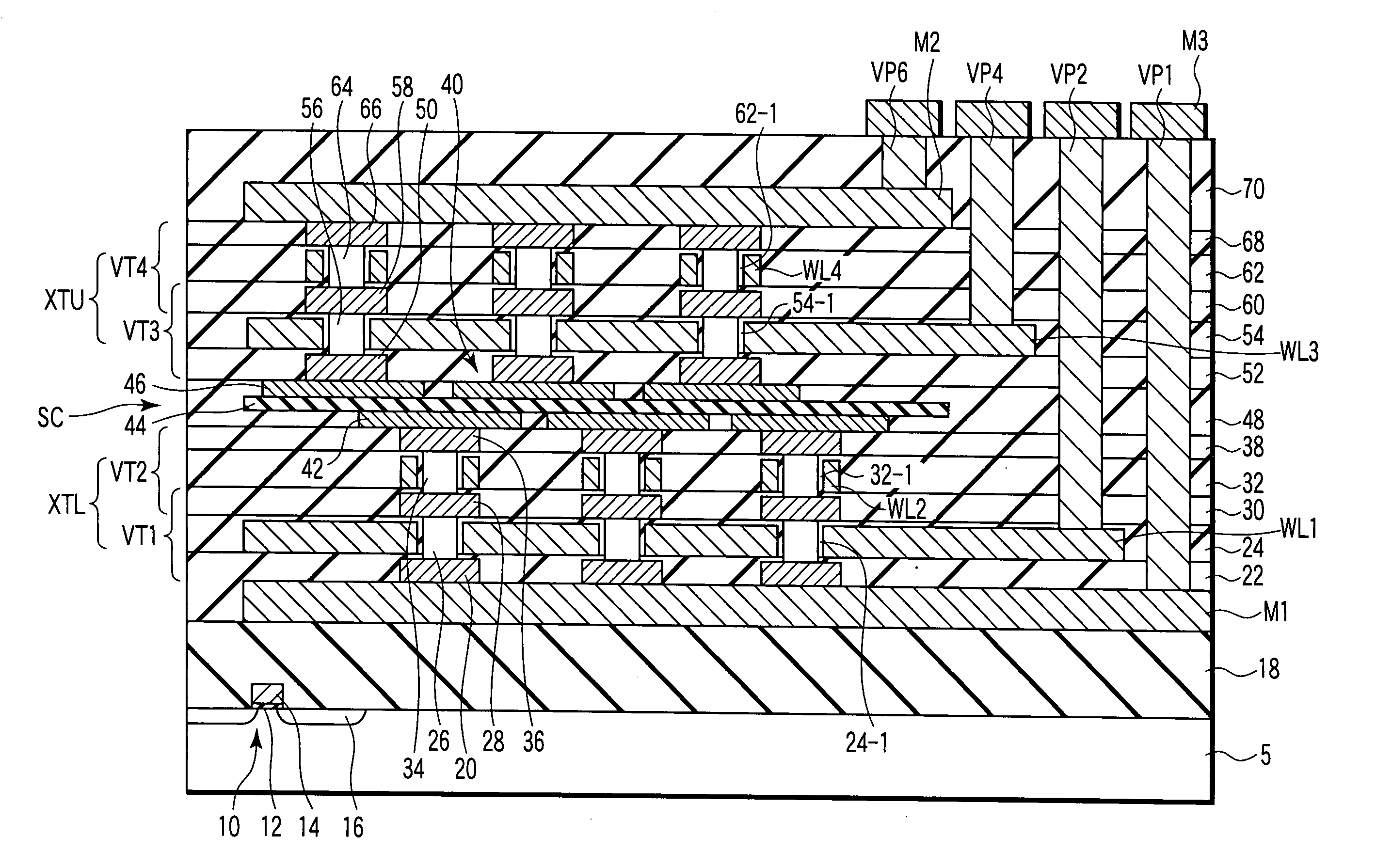
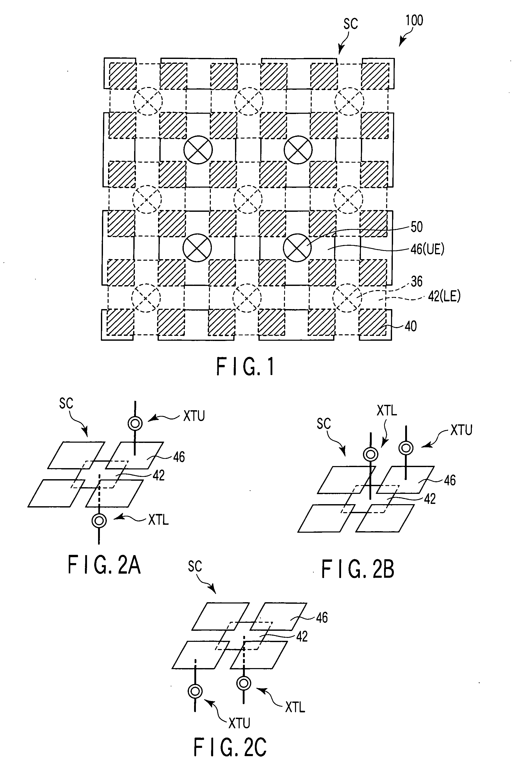
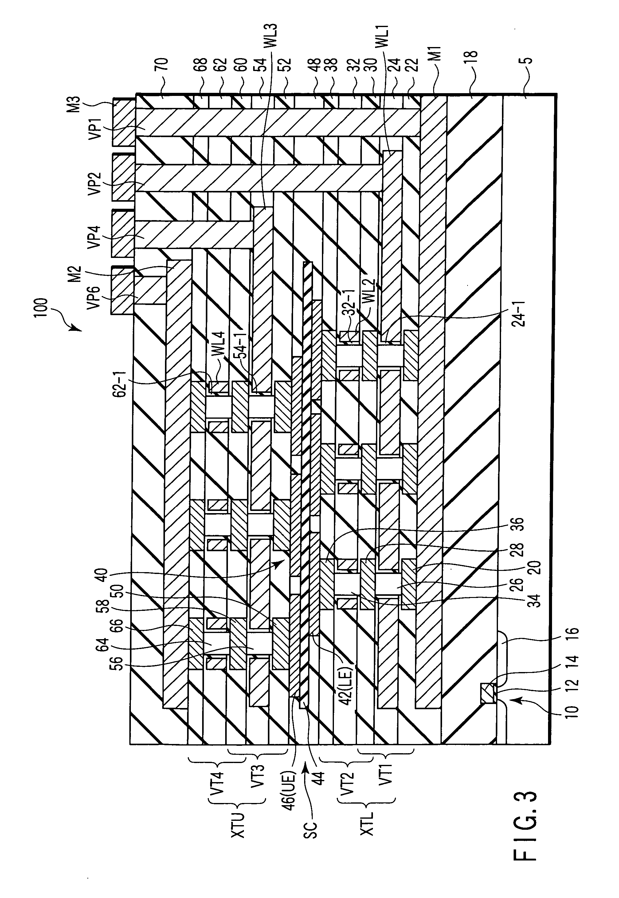
[0023]FIG. 1 is a plan diagram showing an example of a ferroelectric semiconductor memory device 100 according to a first embodiment of the present invention. FIG. 1 shows arrangement of an upper and lower electrodes LE(42) and UE(46) of a ferroelectric capacitor 40. The ferroelectric memory device 100 of the embodiment includes a staggered-electrode capacitor SC. Here, the staggered-electrode capacitor SC refers to a ferroelectric capacitor in which an upper electrode UE of the capacitor 40 is shifted in position with respect to a lower electrode LE. In this structure, if sizes of the lower and upper electrodes LE and UE are set to L×L defined by a minimum feature size L of lithography, an amount of the shift is L / 2 in vertically and horizontally in the drawing, respectively. Arranging the upper electrode UE in such a manner, each about ¼-electrode area of four upper electrodes UE overlaps on one lower electrode LE. Thus, four capacitors 40 are formed on one lower electrode LE in r...

second embodiment

[0070] A semiconductor memory device 200 according to a second embodiment of the present invention has a chain type memory cell comprising a staggered-electrode capacitor SC. An example of the semiconductor memory cell 200 of the embodiment will be described by referring to FIGS. 8A and 8B. FIG. 8A is a plan diagram, and FIG. 8B is a sectional diagram in a serially connected chain-direction cut along a line 8B-8B in FIG. 8A.

[0071] In the chain type memory cell, a capacitor 40 and a MOS transistor 10 are electrically connected in parallel. For the capacitor 40, for example, a ferroelectric capacitor can be used. According to the embodiment, as shown in FIG. 8B, two capacitors 40a, 40b are formed on one lower electrode 42a. For example, the lower electrode 42a is connected with one source / drain 16a of a MOS transistor 10a through a first contact plug 84. An upper electrode 46a is formed by being shifted from the lower electrode 42 by a ½ pitch, and connected with two capacitors 40b, ...

third embodiment

[0077] A semiconductor memory device according to a third embodiment of the present invention includes a ferroelectric capacitor having a hexagonal lower electrode and is a capacitor on bit line (COB) type semiconductor memory device. This structure enables to achieve a higher packing density of the semiconductor memory device. When hexagons are closely packed, each center thereof is shifted by a ½ pitch in both horizontal and longitudinal directions. The embodiment provides a structure suited to an operation in a 2 transistor-2 capacitor (2T-2C) mode. However, the device can also be operated in a 1 transistor-1 capacitor (1T-1T) mode.

[0078]FIGS. 9A to 9C show an example of a structure of the semiconductor memory device 300 of the embodiment. FIG. 9A is a plan diagram, FIG. 9B is a sectional diagram including a transistor cut along a line 9B-9B in FIG. 9A, and FIG. 9C is a sectional diagram on a bit line BL cut along a line 9C-9C in FIG. 9A.

[0079] The semiconductor memory device 3...


PUM


Abstract

A semiconductor memory device including a capacitor array having an effective size smaller than a minimum feature size of lithography is disclosed. According to one aspect of the present invention, it is provided a semiconductor memory device comprising a transistor including a gate electrode formed on a gate insulator on a semiconductor substrate and a plurality of sources / drains disposed in the semiconductor substrate to face each other holding the gate electrode therebetween, a ferroelectric capacitor formed above the transistor and including a lower electrode, a ferroelectric film, and an upper electrode, a first wiring line electrically connected to the lower electrode, and a second wiring line electrically connected to the upper electrode, wherein the ferroelectric capacitor is a staggered-electrode capacitor in which the upper electrode is shifted from the lower electrode and equivalently overlaps with parts of the plurality of lower electrodes.

Description

CROSS-REFERENCE TO RELATED APPLICATIONS [0001] This application is based upon and claims the benefit of priority from prior Japanese Patent Application No. 2006-092097, filed Mar. 29, 2006, the entire contents of which are incorporated herein by reference. BACKGROUND OF THE INVENTION [0002] 1. Field of the Invention [0003] The present invention relates to a semiconductor memory device, and more particularly to a semiconductor memory device including a capacitor. [0004] 2. Description of the Related Art [0005] Higher integration of a semiconductor device has been accompanied by a progress in miniaturization of elements used for the semiconductor device. The miniaturization of the elements is achieved by reducing a minimum feature size of lithography. [0006] However, current semiconductor devices are not enough to satisfy a demand for miniaturization. For example, as disclosed in Jpn. Pat. Appln, KOKAI Publication No. 2001-257320, in a semiconductor memory device such as a ferroelectr...

Claims


Application Information

Patent Timeline
Patent Type & Authority Applications(United States)
IPC IPC(8): H01L29/94H01L27/108H01L29/76H01L31/119
CPCG11C5/02G11C11/22H01L27/0203H01L28/55H01L27/11502H01L27/11507H01L27/0688H10B53/30H10B53/00
Inventor SHIMOJO, YOSHIRO
Owner KK TOSHIBA
Why Eureka
Try Eureka