Semiconductor radiation source and light curing device

a radiation source and semiconductor technology, applied in the field of semiconductor radiation sources, can solve the problems of insufficient cooling, unsatisfactory, and often exhibit uneven power distribution, and achieve the effect of improving the calibration resul

Inactive Publication Date: 2007-10-04
IVOCLAR VIVADENT AG
View PDF15 Cites 25 Cited by
  • Summary
  • Abstract
  • Description
  • Claims
  • Application Information

AI Technical Summary

Benefits of technology

[0010]The inventive measure of arranging series resistors for the LED chips on a printed circuit board surprisingly results in a greatly improved calibration result. It is obviously important for the calibration accuracy that the series resistors are not subjected to excessive temperature fluctuations especially since carbon film resistors have a negative temperature coefficient, i.e. the resistance value of resistance layers which are intended to be small becomes even smaller as a result of heating and thus becomes too small.

Problems solved by technology

On the other hand, this raises the problem of sufficient cooling especially in the case of high-power light-emitting diodes and LED chips.
During operation, LED chips of this type nevertheless frequently exhibit an uneven power distribution which is unsatisfactory and could not really be eliminated even by repeated readjustment.

Method used


Image

  • Semiconductor radiation source and light curing device
  • Semiconductor radiation source and light curing device
  • Semiconductor radiation source and light curing device

Examples


Embodiment Construction

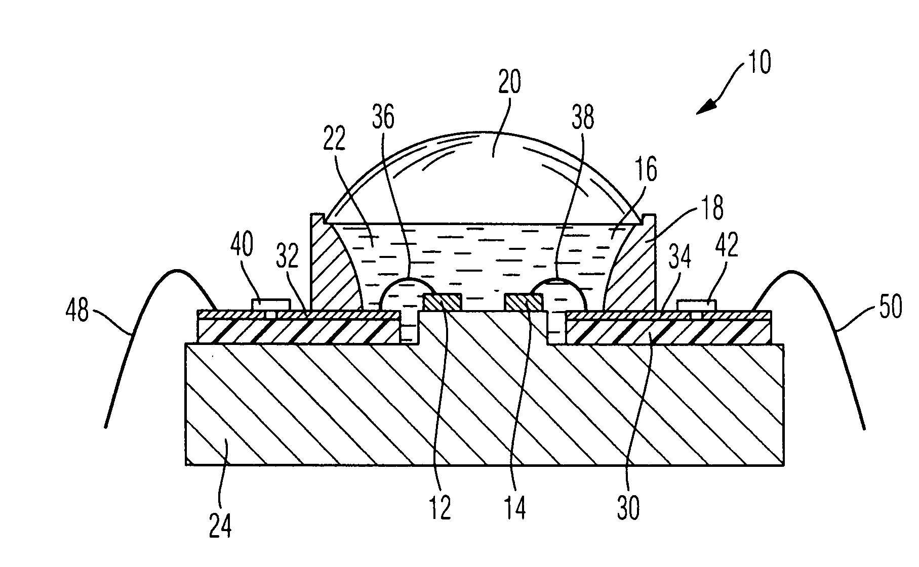
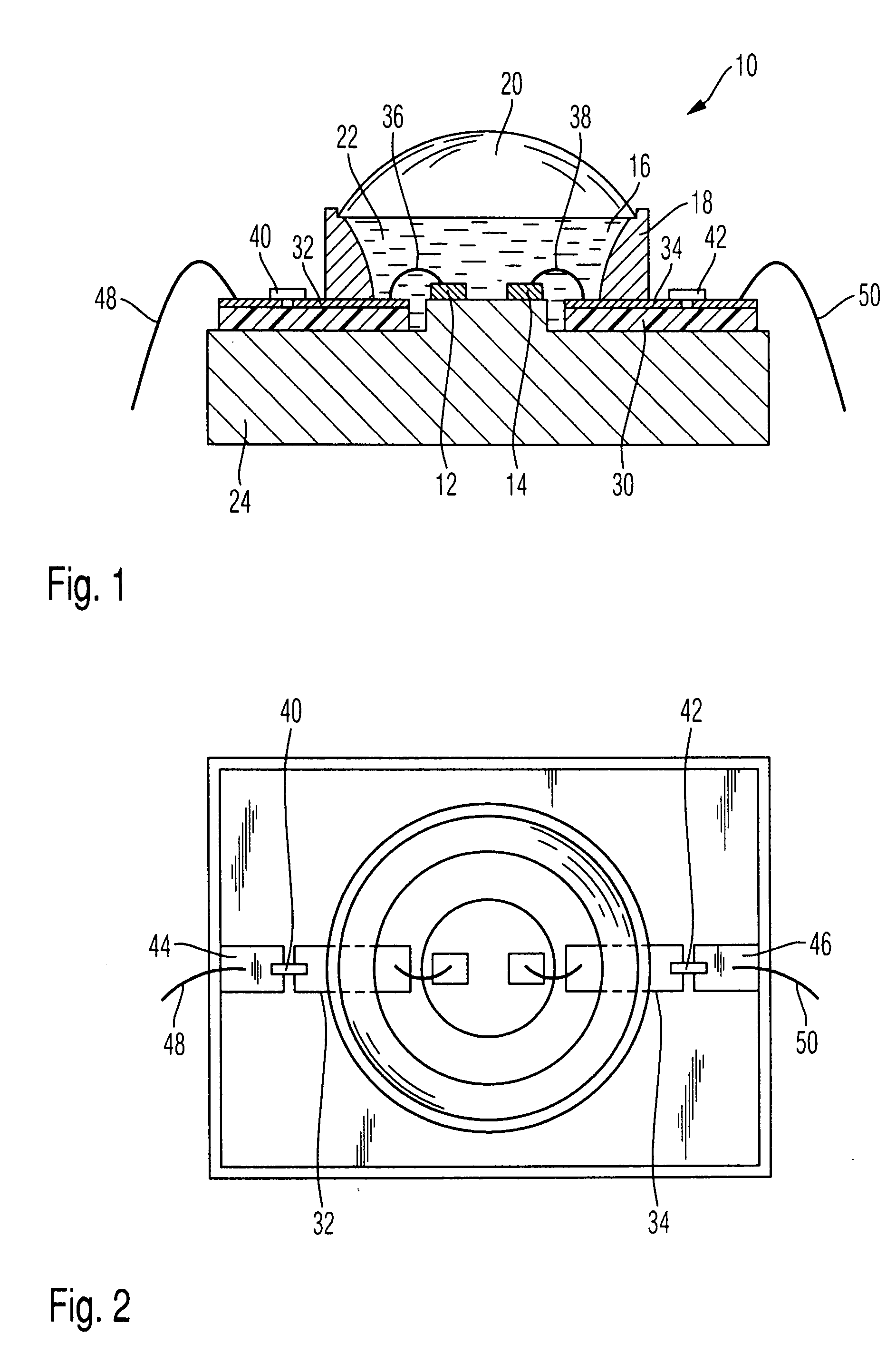
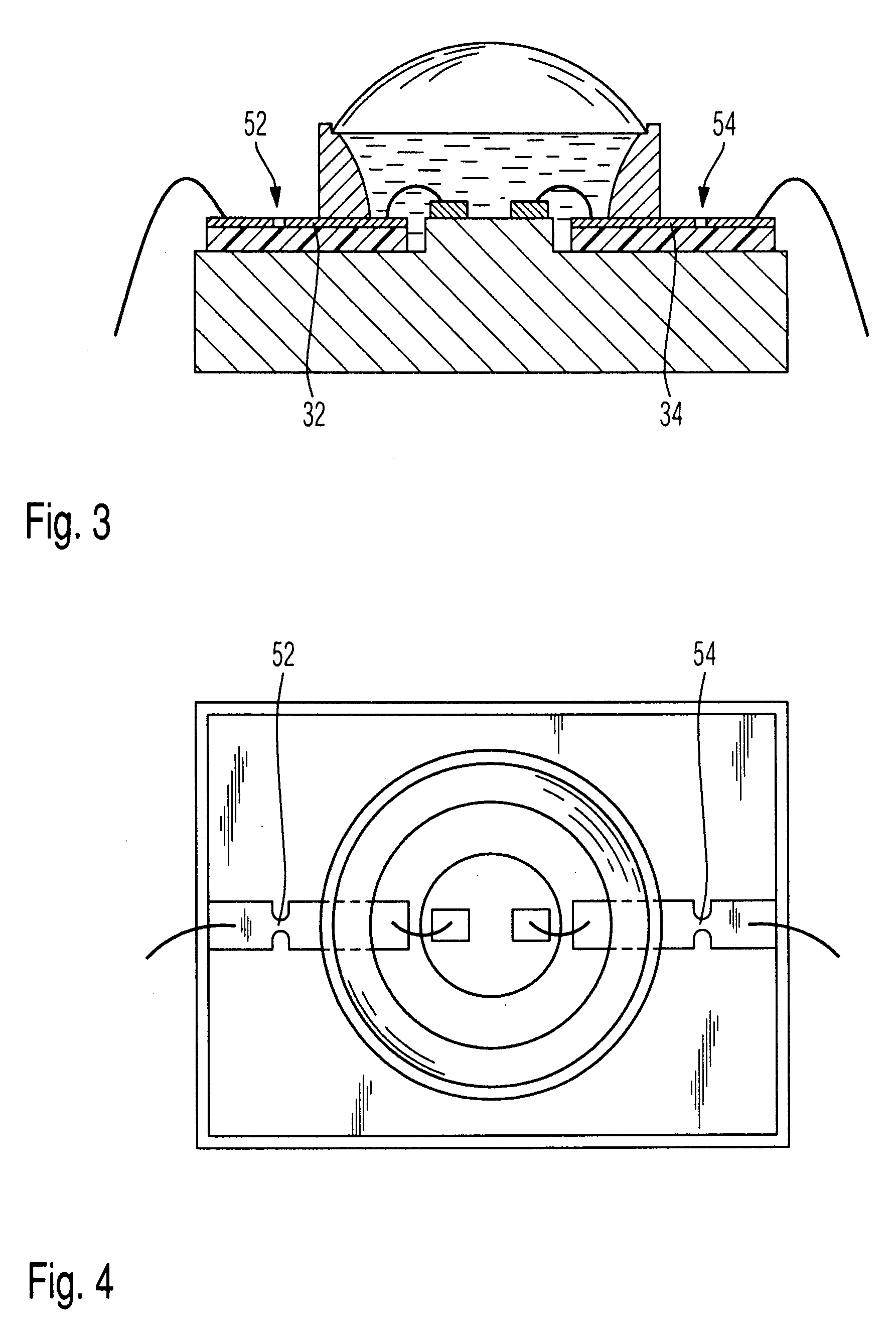
[0063]The semiconductor radiation source 10 illustrated in FIG. 1 has a plurality of LED chips 12, 14 (two chips in the exemplary embodiment illustrated). The chips are held in an internal space 16 which is surrounded by a supporting element 18 for a lens 20. The lens 20 is mounted and sealed on a circumferential bearing shoulder of the supporting element. In the exemplary embodiment illustrated, the internal space 16 is filled with a transparent medium 22.

[0064]The LED chips 12, 14 are permanently fitted to a base body 24 using a thermally conductive connection. The base body may be composed of copper, for example, and the chips may be adhesively bonded using an adhesive having a strength of a few micrometers, with the result that there is an extremely low thermal resistance which also permits high-power LED chips.

[0065]The invention provides for the LED chips 12 and 14 to be arranged such that they are surrounded by a printed circuit board. The printed circuit board is fastened to...


PUM


Abstract

Provision is made of a semiconductor radiation source having a base body on which at least two LED chips are mounted, at least one chip of which is connected to a series resistor which can be adjusted. The LED chips (12, 14) are fitted to the base body (24) using a thermally conductive connection and at least one printed circuit board (30) which bears the series resistor (40, 42) is also mounted on the base body (24).

Description

CROSS-REFERENCE TO RELATED APPLICATIONS[0001]This application claims foreign priority benefits under 35 U.S.C. §119 from German patent application Ser. No. 10 2006 015 335.9 filed Apr. 3, 2006.TECHNICAL FIELD[0002]The invention relates to a semiconductor radiation source having a base body on which at least two LED chips are mounted, and, more particularly to a semiconductor radiation source having at least two LED chips wherein at least one chip is connected to a series resistor which can be adjusted.BACKGROUND OF THE INVENTION[0003]Semiconductor radiation sources have been known for a long time. They may have light-emitting diodes or LEDs whose emission spectrum can be adapted to the requirements as regards the sensitivity spectrum of the materials to be cured by appropriately selecting the LEDs.[0004]Light curing devices must be calibrated, as has already been disclosed, for example, in U.S. Pat. No. 6,095,812. On the other hand, the practice of calibrating light-emitting diodes,...

Claims


Application Information

Patent Timeline
Patent Type & Authority Applications(United States)
IPC IPC(8): H01L29/00H01L33/64
CPCA61C19/003F21K9/00H01L25/0753H01L25/167H01L33/64H01L2924/3025H01L2924/19107H01L2224/48091H01L2924/00014H01L2924/00H01L2924/181H01L33/60H01L33/62H01L2924/00012
Inventor PLANK, WOLFGANGSENN, BRUNO
Owner IVOCLAR VIVADENT AG
Why Eureka
Try Eureka