System and method for DC offset compensation and bit synchronization

a bit synchronization and offset compensation technology, applied in the field of wireless communication devices and protocols, can solve the problems of affecting the synchronization frame system, unable to meet the dc level restoring means or bias distort correction, and the system details of the baseband system, etc., to achieve the effect of preventing bit slippag

Inactive Publication Date: 2007-10-04
AVAGO TECH INT SALES PTE LTD
View PDF18 Cites 0 Cited by
  • Summary
  • Abstract
  • Description
  • Claims
  • Application Information

AI Technical Summary

Benefits of technology

[0011] The DC tracking loop, for example, can be a digital emulation of a cascade of two analog one-pole LPFs (low pass filters). The DC tracking loop provides flexibility and stability when compared to conventional one-pole LPFs. Additionally, the DC tracking loop can include a variable time constant to provide responsiveness to DC variations caused by frequency drift over time. The output of the DC tracking loop is a DC offset estimate that can account for long term drift and short term fluctuations.
[0014] To overcome long timing drift or random timing jitter causing bit slippage, when the maximum averaged sample sum amplitude is not from the optimal, i.e., an on-time hypothesis, the MHBS can apply a timing control logic to recenter the next symbol time. Assuming that the sample rate is N samples per symbol, when a late hypothesis corresponds to the maximum averaged sample sum, the next symbol time is (N+1) samples later rather than N. Similarly, if an early hypothesis corresponds to the maximum averaged sample sum, the next symbol time is (N−1) samples later. Thus, the MHBS recenters the symbol window in both cases, thereby preventing bit slippage.

Problems solved by technology

Present devices compensate for DC-related imperfections in incoming signals using a variety of means, none of which are completely satisfactory.
Present technology suffers drawbacks in addition to those described above.
Present systems for synchronizing frames are slow, require significant hardware, and are not entirely accurate.
Accordingly, present systems can waste valuable time and unnecessarily drop frames.
Although present analog and digital approaches to computing DC offsets and synchronizing frames for wireless communications are functional, they are not sufficiently accurate or otherwise satisfactory.

Method used


Image

  • System and method for DC offset compensation and bit synchronization
  • System and method for DC offset compensation and bit synchronization
  • System and method for DC offset compensation and bit synchronization

Examples


Embodiment Construction

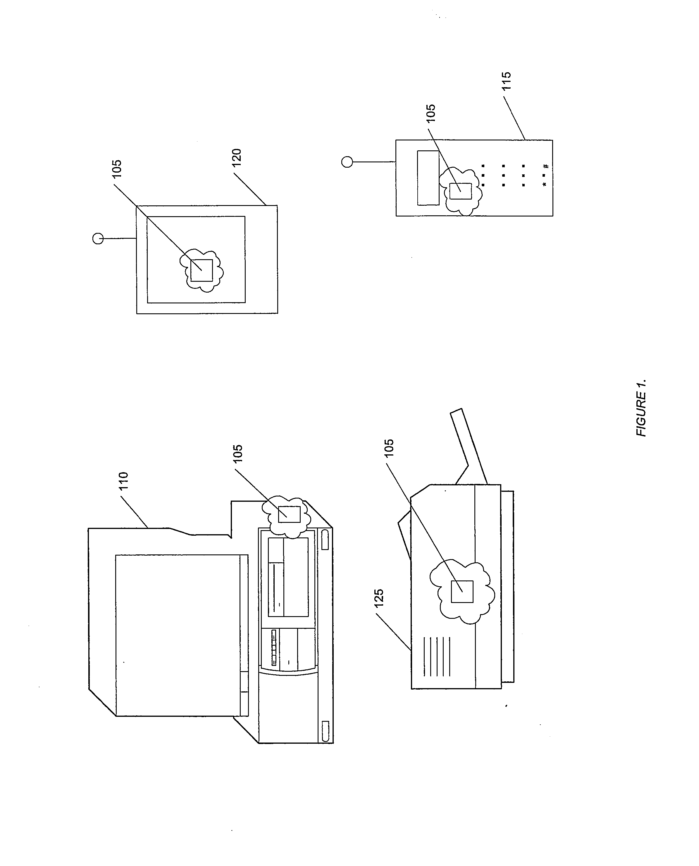
[0025] Referring now to the drawings, where like or similar elements are designated with identical reference numerals throughout the several views, and referring in particular to FIG. 1, it illustrates examples of electronic devices with integrated receiver modules 105 constructed in accordance with the principles of the present invention. The receiver modules 105 can be implemented in a variety of ways, and preferred implementations of the receiver modules 105 are discussed in detail herein.

[0026] Although only a computer 110, a PDA (personal digital assistant) 115, cell phone 120 and peripheral device 125 are illustrated, implementations of the present invention can include any type of wireless-enabled device and should not be limited to those devices shown. Moreover, the receiver modules 105 in these various devices can include, for example, ASICs (application specific integrated circuits), software instructions, general purpose processors, or any combination thereof.

[0027]FIG....


PUM


Abstract

A system and method for compensating for DC offset and / or clock drift on a wireless-enabled device is described. One embodiment includes a radio module, an A / D converter connected to the radio module, a DC tracking loop connected to the A / D converter, and a multi-hypothesis bit synchronizer.

Description

RELATED APPLICATIONS [0001] The present application is related to commonly owned and assigned Attorney Docket No. WIDC-023 / 00US, entitled Bluetooth Access Code Assisted Initial DC Estimation and Frame Synchronization, which is filed on even date herewith and is incorporated herein by reference. FIELD OF THE INVENTION [0002] The present invention relates to wireless communication devices and protocols. In particular, but not by way of limitation, the present invention relates to systems and methods for improving the quality and commercial appeal of wireless communications and wireless communication devices. BACKGROUND OF THE INVENTION [0003] Wireless communications and wireless communication devices are at the center of many important technological advancements. As the proliferation of these wireless devices increases, the efficiency and accuracy of the communications therebetween becomes vital to the commercial success of particular devices and particular communication protocols. On...

Claims


Application Information

Patent Timeline
Patent Type & Authority Applications(United States)
IPC IPC(8): H04L25/10H03M1/06H03M1/12H04L7/02H04L25/06
CPCH03M1/0607H04L25/061H04L7/007H03M1/12
Inventor YUAN, REBECCA W.
Owner AVAGO TECH INT SALES PTE LTD
Why Eureka
Try Eureka