Integrated Circuit and Metod for Issuing Transactions

a technology of integrated circuits and transactions, applied in the field of integrated circuits, can solve the problems of large number of modules forming a large bus load, system complexity on silicon shows a continuous increase in complexity, and achieve the effect of reducing the time a resource is locked

Inactive Publication Date: 2007-10-04
KONINKLIJKE PHILIPS ELECTRONICS NV
View PDF13 Cites 33 Cited by
  • Summary
  • Abstract
  • Description
  • Claims
  • Application Information

AI Technical Summary

Benefits of technology

[0030] The invention is based on the idea to reduce the time a resource is locked or is flagged with exclusive access to a minimum b

Problems solved by technology

Systems on silicon show a continuous increase in complexity due to the ever increasing need for implementing new features and improvements of existing functions.
As the number of modules increases however, this way of communication is no longer practical for the following reasons.
On the one hand the large number of modules forms a too high bus load.
On the other hand the bus forms a communication bottleneck as it enables only one device to send data to the bus.
Using networks for on-chip communication when designing systems on chip (SoC), however, raises a number of new issues that must be taken into account.
However, NoC's premises are different from off-chip networks, and, therefore, most of the network design choices must be reevaluated.
On-chip networks have different properties (e.g., tighter link synchronization) and constraints (e.g., higher memory cost) leading to different design choices, which ultimately affect the network services.
Storage (i.e., memory) and computation resources are relatively more expensive, whereas the number of point-to-point links is larger on chip than off chip .
Storage is expensive, because general- purpose on-chip memory, such as RAMs, occupy a large area.
Having the memory distributed in the network components in relatively small sizes is even worse, as the overhead area in the memory then becomes dominant.
For on-chip networks computation too comes at a relatively high cost compared to off-chip networks.
Including a dedicated processor in a network interface is not feasible on chip, as the size of the network interface will become comparable to or larger than the IP to be connected to the network.
Moreover, running the protocol stack on the IP itself may also be not feasible, because often these IPs have one dedicated function only, and do not have the capa

Method used


Image

  • Integrated Circuit and Metod for Issuing Transactions
  • Integrated Circuit and Metod for Issuing Transactions
  • Integrated Circuit and Metod for Issuing Transactions

Examples


first embodiment

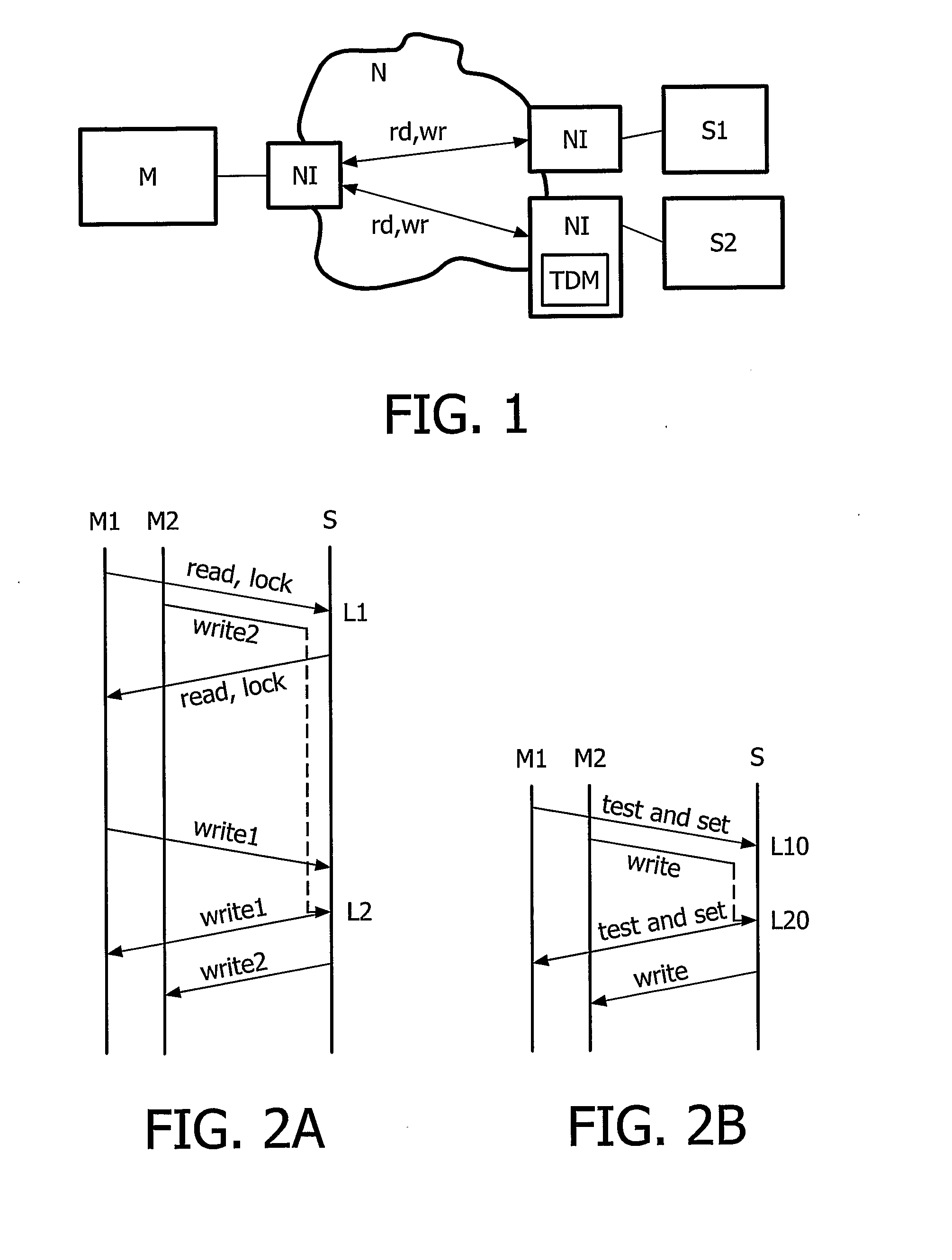
[0042] An implementation thereof is illustrated in FIGS. 2A and 2B. A traditional atomic operation using locking is shown in FIG. 2A, and the atomic operation is shown in FIG. 2B.

[0043] Therefore, FIG. 2A shows a basic representation of a communication scheme between a first and second master M1, M2 and a slave S within a network on chip environment. The first master M1 requests a ‘read & lock’ operation, i.e. read a value in the slave S and lock the slave S, and the slave S returns a response ‘read & lock’, possibly returning a read value. The slave S is then locked (L1) to the master M1 so that a request ‘write2’ from the second master M2 is blocked, i.e. its execution is delayed. After the master M1 received the response ‘read & lock’ from the slave S, it issues a request ‘write1’ to the slave S in order to write a value into the slave S. This second request from the master M1 is received by the slave S and a response ‘write1’ is forwarded to the master M1 and the locking of the...

second embodiment

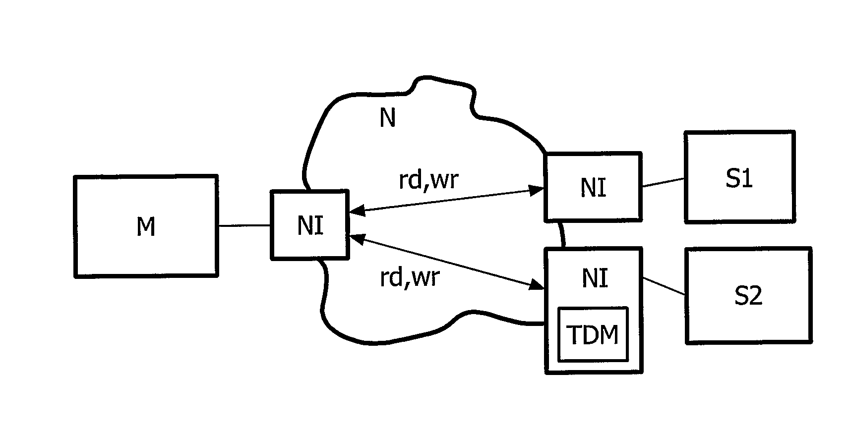
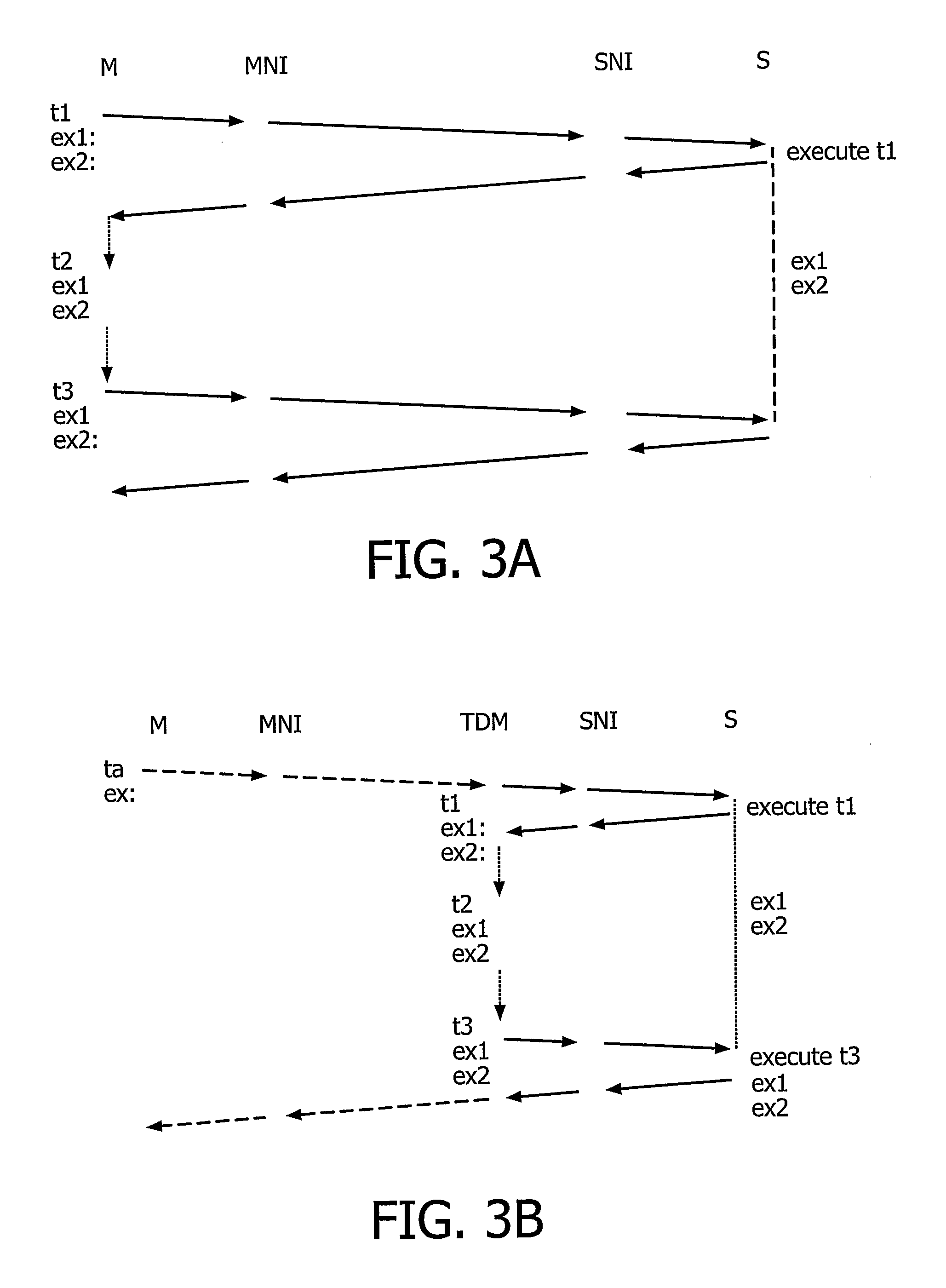
[0050] In FIG. 3B a basic representation of a communication scheme between a master M and a slave S within a network on chip environment is shown according to the The basic structure of the underlying network on chip environment corresponds to the environment as described in FIG. 3A, however a transaction decoding means TDM is additionally included into the network on chip environment. The master M issues an atomic transaction ta like a TestAndSet which is forwarded to the transaction decoding means TDM via the network interface MNI of the master M.

[0051] As described according to FIG. 3A two different execution examples for implementations or decoding of the atomic transaction ta of a TestAndSet command are described, namely LockedRead and Write as first execution example ex1 and ReadLinked and WriteConditional as second execution example ex2.

[0052] Here, the master M issues an atomic transaction ta. The decoding of the atomic transaction ta and the processing of first, second an...


PUM


Abstract

An integrated circuit is provided comprising a plurality of processing modules (M, S) and a network (N) arranged for coupling said processing modules (M, S). Said integrated circuit comprises a first processing module (M) for encoding an atomic operation into a first transaction and for issuing said first transaction to at least one second processing module (S) . In addition, a transaction decoding means (TDM) for decoding the issued first transaction into at least one second transaction is provided.

Description

FIELD OF THE INVENTION [0001] The invention relates to an integrated circuit having a plurality of processing modules and a network arranged for providing connections between processing modules, a method for issuing transactions in such an integrated circuit, and a data processing system. BACKGROUND OF THE INVENTION [0002] Systems on silicon show a continuous increase in complexity due to the ever increasing need for implementing new features and improvements of existing functions. This is enabled by the increasing density with which components can be integrated on an integrated circuit. At the same time the clock speed at which circuits are operated tends to increase too. The higher clock speed in combination with the increased density of components has reduced the area which can operate synchronously within the same clock domain. This has created the need for a modular approach. According to such an approach the processing system comprises a plurality of relatively independent, co...

Claims


Application Information

Patent Timeline
IPC IPC(8): G06F15/76G06F15/78
CPCG06F15/7825G06F15/78G06F15/173H04L12/28
Inventor RADULESCU, ANDREIGOOSSENS, KEES GERARD WILLEM
Owner KONINKLIJKE PHILIPS ELECTRONICS NV
Why Eureka
Try Eureka