
Organic light-emitting diodes with nanostructure film electrode(s)

a light-emitting diode and nano-structure film technology, applied in the manufacture of electrode systems, electric discharge tubes/lamps, discharge tubes luminescnet screens, etc., can solve the problems of high cost, high cost, and high cost of ito, and achieves relatively low work function and corrosion resistance. , the effect of reducing the number of defects

Inactive Publication Date: 2007-10-11
RGT UNIV OF CALIFORNIA +1
View PDF11 Cites 11 Cited by
  • Summary
  • Abstract
  • Description
  • Claims
  • Application Information

AI Technical Summary

Benefits of technology

[0015] Other features and advantages of the invention will be apparent from the accompanying drawings and from the detailed description. One or more of the above-disclosed embodime...

Problems solved by technology

However, ITO, with its relatively brittle structure, can be an inadequate solution for many emerging applications (e.g., flexible optoelectronic devices such as many OLEDs), and the indium component of ITO is rapidly becoming a scarce commodity.
Moreover, ITO has significant limitations for current and future generations of OLEDs, including diffusion of oxygen into proximate organic charge transporting / emissive layers, significant absorption in the blue region, a relatively low work function and corrosion susceptibility.

Method used


Image

  • Organic light-emitting diodes with nanostructure film electrode(s)
  • Organic light-emitting diodes with nanostructure film electrode(s)
  • Organic light-emitting diodes with nanostructure film electrode(s)

Examples


Embodiment Construction

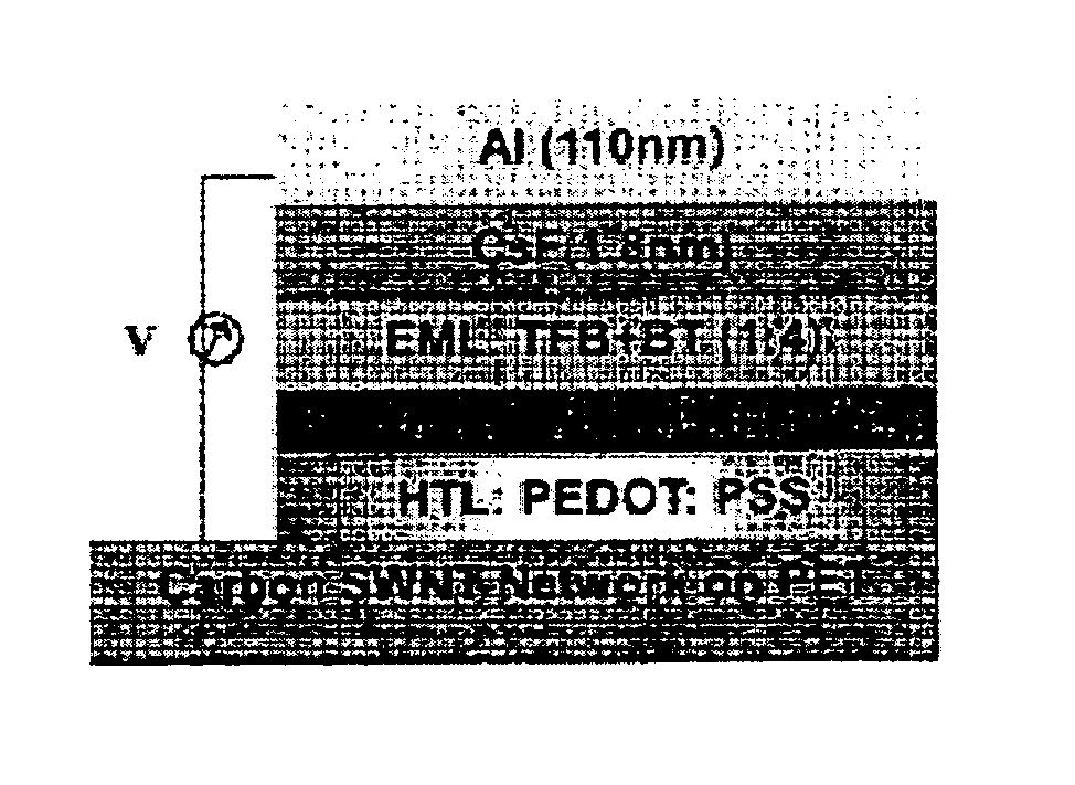
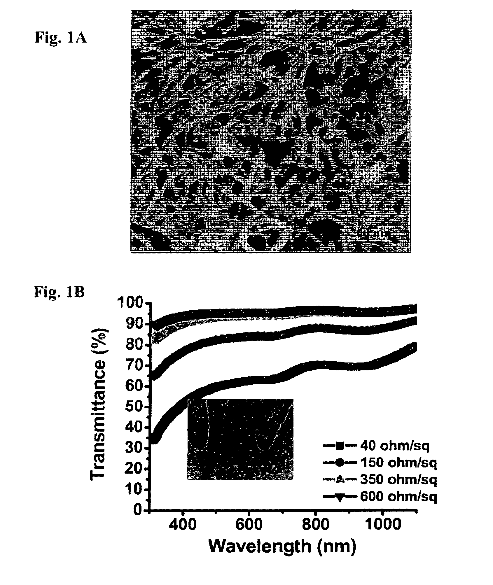
[0028] Referring to FIG. 1A, a nanostructure-film according an embodiment of the present invention comprises a two-dimensional random network of nanostructures. This film is preferably at least semi-transparent and electrically conductive, and preferably comprises at least one network of single-walled carbon nanotubes (SWNTs).

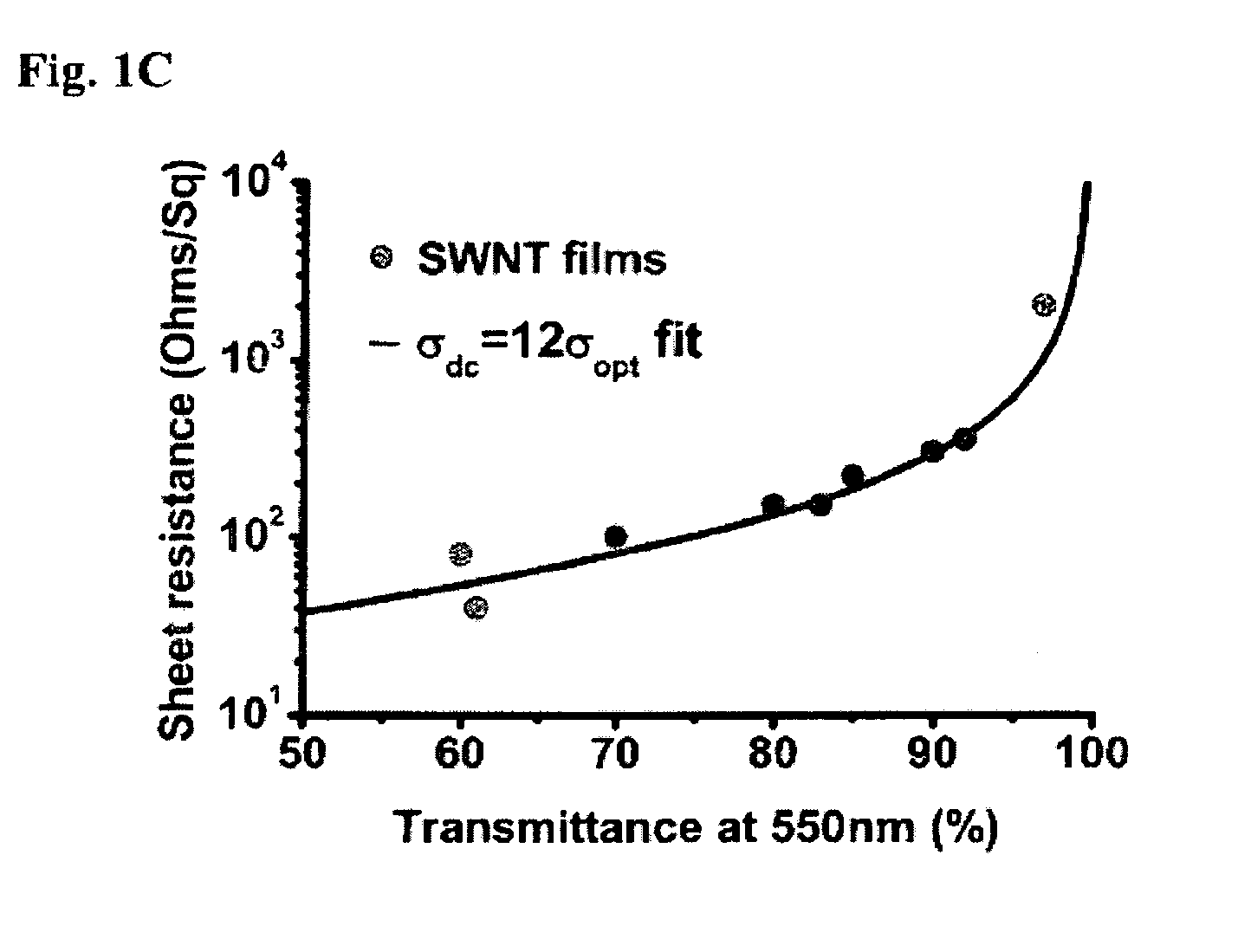
[0029] Transparent conducting nanostructure-films composed of randomly distributed SWNTs (i.e., networks) have been demonstrated as substantially more mechanically robust than ITO. Additionally, theoretical and experimental studies have established that the work function of SWNT networks can be in the range of 4.7-5.2 eV—sufficiently high to meet at least the anode requirements for such optoelectronic devices as OLEDs. Moreover, SWNTs can be deposited using a variety of low-impact methods (e.g., it can be solution processed), and comprise carbon, which is one of the most abundant elements on Earth.

[0030] SWNT networks may be fabricated by, for example, suspen...


PUM


Abstract

Organic light-emitting diodes (OLEDs) comprising at least one nanostructure-film electrode, and fabrication methods thereof are discussed. The nanostructure-film is preferably transparent, and may be deposited on a preferably-transparent substrate using a variety of techniques. A different material may be used to planarize the nanostructure-film and / or otherwise improve OLED performance.

Description

[0001] This application claims priority to U.S. Provisional Patent Application No. 60 / 833,789, filed Jul. 28, 2006, and entitled “ORGANIC LIGHT-EMITTING DIODES WITH SINGLE-WALLED CARBON NANOTUBE FILM ANODES,” and PCT Application No. US / 2005 / 047315, filed Dec. 27, 2005, and entitled “COMPONENTS AND DEVICES FORMED USING NANOSCALE MATERIALS AND METHODS OF PRODUCTION,” which are hereby incorporated herein by reference.FIELD OF THE INVENTION [0002] The present invention relates in general to light emitting diodes, and more particularly to an organic light emitting diode comprising a nanostructure-film. BACKGROUND [0003] Polymer-based and small molecule-based organic light-emitting diodes (OLEDs) are rapidly approaching large-scale commercialization, driven by such attractions as low cost, fast response, and applications in large-area flexible displays, as well by recent advances in efficiencies and operational lifetimes. [0004] OLEDs are dual injection devices in which holes and electron...

Claims


Application Information

Patent Timeline
IPC IPC(8): H01J1/62H01J9/00
CPCB82Y10/00H01L51/0048H01L51/5206H01L51/444H01L51/0097H10K85/221H10K30/821H10K77/111H10K50/81
Inventor HU, LIANGBINGGRUNNER, GEORGELI, JIANFENGMARKS, TOBIN
Owner RGT UNIV OF CALIFORNIA
Learn More