Semiconductor Device and Manufacturing Process Therefor

a technology of semiconductors and semiconductors, applied in the direction of semiconductor devices, electrical devices, transistors, etc., can solve the problems of difficult operation of integrated circuits, ingenious dislocations and defects in channel si layers, and significantly difficult to reduce the size of integrated circuits, etc., to achieve less dislocations or defects, improve carrier mobility, and control the effect of strain

Active Publication Date: 2007-10-18
GK BRIDGE 1
View PDF5 Cites 147 Cited by
  • Summary
  • Abstract
  • Description
  • Claims
  • Application Information

AI Technical Summary

Benefits of technology

[0013] An objective of the present invention is to provide a semiconductor device in which carrier mobility is improved by introducing strain by employing a novel structure. Another objective is to provide a semiconductor device with less dislocations or defects and a controlled amount of strain. Another objective is to provide a process for manufacturing such a semiconductor device.
[0036] The present invention utilizes deflection for applied strain to a semiconductor layer. Particularly, by deflecting a beam from a doubly-clamped beam structure, strain is introduced in the beam in proportion to the amount of deflection. In such a structure, strain is introduced differently from a conventional process in which strain is introduced based on lamination of semiconductor layers different in a lattice constant, so that dislocations or defects caused by a lower semiconductor layer are avoided. Thus, it can improve reliability and give a good process yield during production, resulting in a semiconductor device allowing for high speed operation. Unlike the case where strain is introduced by, for example, a capping layer, since strain can be directly controlled by deflection in this structure, this structure has advantage of facilitating designing of a semiconductor device.
[0037] In one aspect of the manufacturing process according to the present invention, since utilizing sticking phenomenon caused by a liquid surface tension while beam is deflected, dislocations or defects can be avoided, resulting in higher reliability and a good process yield. Furthermore, since strain can be easily controlled by deflection, the present invention has advantage of facilitating designing of a semiconductor device.

Problems solved by technology

Recently, it has become significantly difficult to reduce the size of an integrated circuit in accordance with the scaling rule.
However, a relaxed SiGe layer giving strain to a channel Si layer has many dislocations and defects, so that it transfers dislocations and defects to the channel Si layer, leading to tendency to ingenerate dislocations and defects in the channel Si layer.
Thus, when using the first method, a single MOS transistor may operate while it is difficult to operate an integrated circuit.
Even if the integrated circuit operates, it is difficult to ensure a process yield.
However, in the second method, strain is hard to be directly applied to a channel and it is difficult to control the amount of strain.

Method used


Image

  • Semiconductor Device and Manufacturing Process Therefor
  • Semiconductor Device and Manufacturing Process Therefor
  • Semiconductor Device and Manufacturing Process Therefor

Examples


embodiment 1

Modification of Embodiment 1

[0113] In the process of the present invention, different strain can be applied to each FinFET constituting an integrated circuit. For example, when a certain FinFET is to be used as a conventional FinFET without strain, the FinFET can be masked after the process of FIG. 3, not to be etched during the buried oxide film etching in FIG. 4. Since the strain amount can be controlled by L and d as described above, under a constant d condition, strain can be controlled by altering L for each FinFET. Under a constant L condition, the amount of buried oxide film etching d is altered for each FinFET. That is, buried oxide film etching is conducted more than once appropriately in combination with masking of a FinFET, to apply different strain to each FinFET. These methods can be combined.

[0114] For example, a triple gate type FinFET is layouted such that the Fin in parallel to the X-axis using a (100) SOI wafer and keeping a notch down. Here, the upper surface of...

embodiment 2

[0116] There will be described Embodiment 2 of the present invention with reference to the drawings.

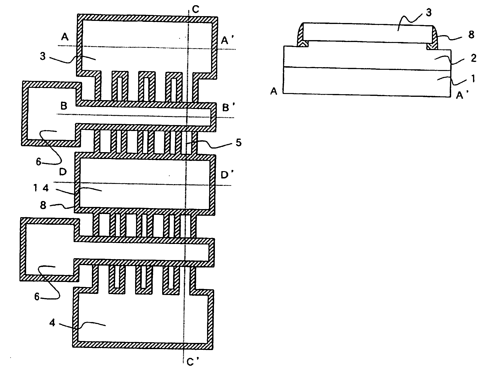
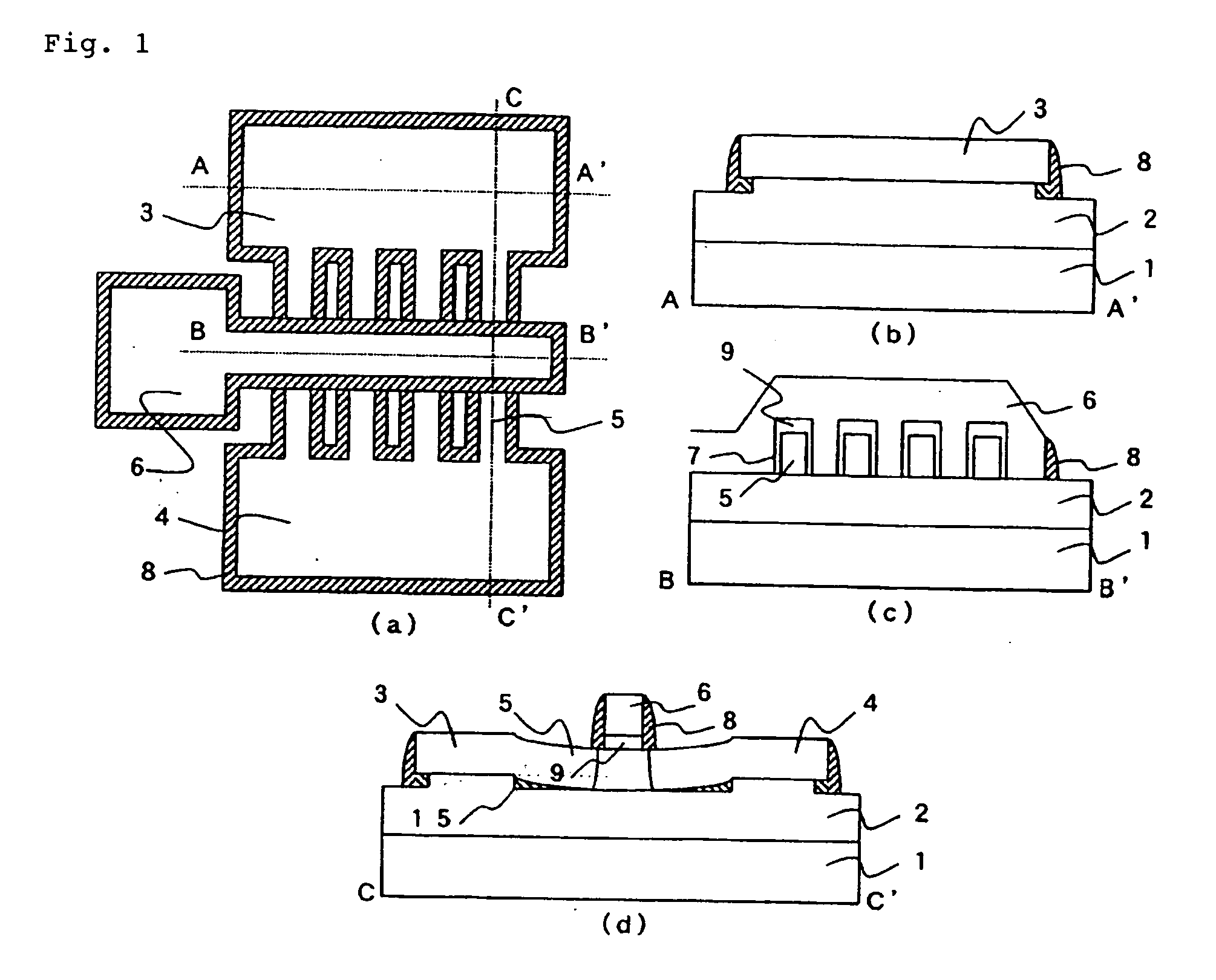
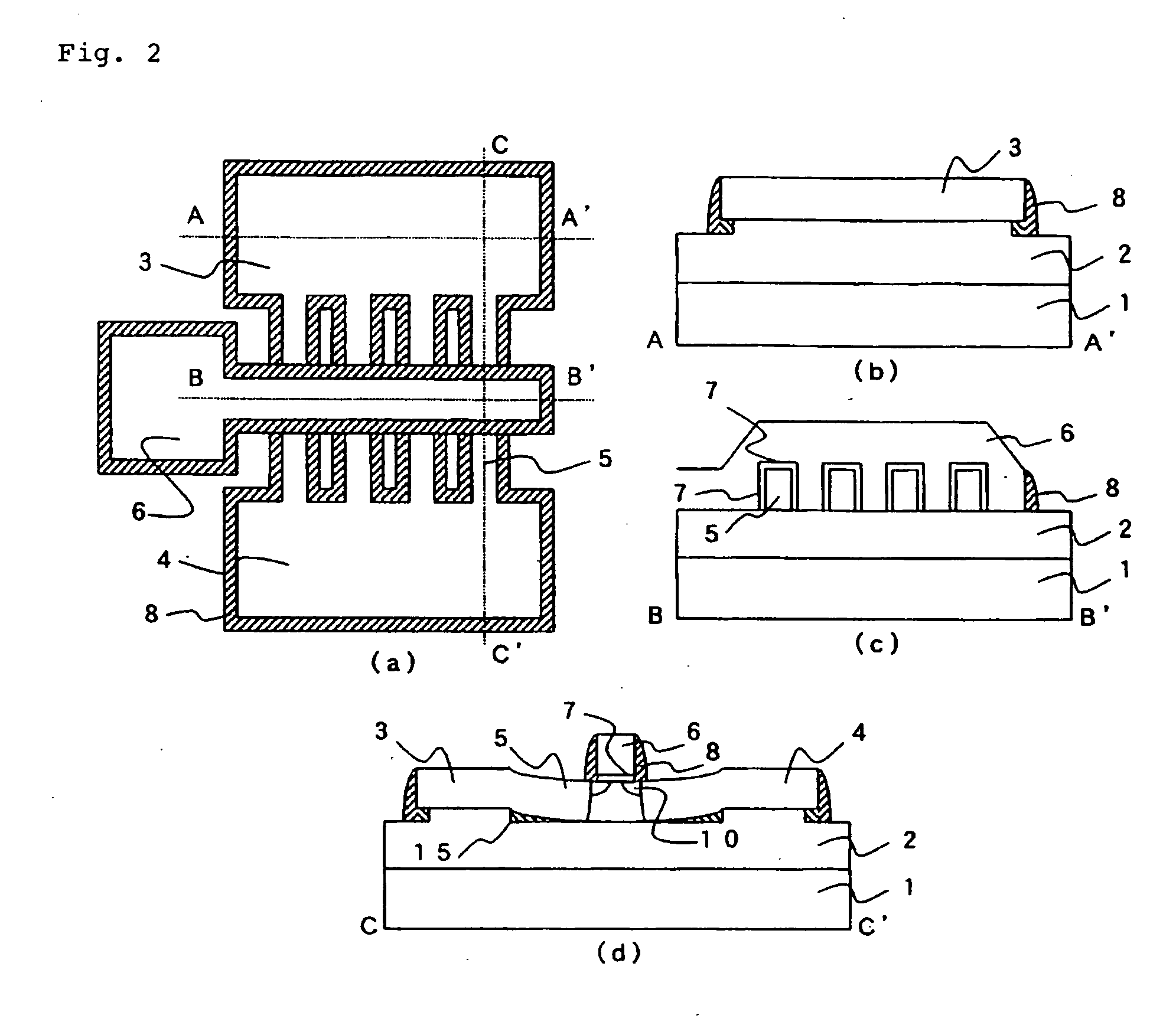
[0117]FIGS. 11 and 12 schematically show Embodiment 2 of a semiconductor device of the present invention. FIG. 11(a) is a top view, and FIGS. 11(b), (c) and (d) are cross-sectional views taken on lines A-A′, B-B′ and C-C′ of FIG. 11(a), respectively. FIG. 12(a) is a top view, and FIGS. 12(b), (c) and (d) are cross-sectional views taken on lines A-A′, B-B′ and C-C′ of FIG. 12(a). FIG. 11 shows a double-gate type FinFET before forming a silicide. FIG. 12 shows a triple gate type FinFET before forming a silicide.

[0118] Embodiment 2 employs a manufacturing process different from that in Embodiment 1, in which steps are reduced. Reflecting the difference, the structures are partly different. Specific differences are a shape of the gate electrode 6 and an insulating film under the fin 5. The gate electrode 6 in Embodiment 2 has a so-called notch type gate shape where a region in contact w...

embodiment 3

[0130] Next, there will be described Embodiment 3 of the present invention with reference to the drawings.

[0131]FIGS. 16 and 17 schematically show Embodiment 3 of a semiconductor device of the present invention. FIG. 16(a) is a top view, and FIGS. 16(b), (c) and (d) are cross-sectional views taken on lines A-A′, B-B′ and C-C′ of FIG. 16(a), respectively. FIG. 17(a) is a top view, and FIGS. 17(b), (c) and (d) are cross-sectional views taken on lines A-A′, B-B′ and C-C′ of FIG. 17(a). FIG. 16 shows a double-gate type FinFET before forming a silicide. FIG. 17 shows a triple gate type FinFET before forming a silicide.

[0132] Embodiment 3 of the present invention is different from Embodiment 1 in a method for forming a pad of the source electrode 3 and a pad of the drain electrode 4. Reflecting the difference, the structures are partly different. A structural difference is that the pad of the source electrode 3 and the pad of the drain electrode 4 are elevated. The structure of the othe...


PUM


Abstract

This invention relates to a semiconductor device having a beam made of a semiconductor to which strain is introduced by deflection, and a current is permitted to flow in the beam.

Description

TECHNICAL FIELD [0001] The present invention relates to a semiconductor device and a manufacturing process therefor, particularly to a semiconductor device in which mobility is improved by strain and a manufacturing process therefor. BACKGROUND OF THE INVENTION [0002] Recently, it has become significantly difficult to reduce the size of an integrated circuit in accordance with the scaling rule. As one of the reasons, it has been difficult to restrain short-channel effect in a MOS (Metal-Oxide-Semiconductor) type FET (Field Effect Transistor) as an elementary element in an integrated circuit. For solving this problem, there has been proposed an FET having a double gate structure (Non-patent reference 1: Applied Physics, The Japan Society of Applied Physics, 2003, Vol. 72 (9), pp. 1136-1142). A double-gate structure FET may have three configurations depending on arrangement of a source electrode, a drain electrode and two gate electrodes as described in Non-patent reference 1, and amo...

Claims


Application Information

Patent Timeline
Patent Type & Authority Applications(United States)
IPC IPC(8): H01L29/78H01L21/336H01L27/12H01L29/786
CPCH01L27/1203H01L29/785H01L29/7842H01L29/66795
Inventor NARIHIRO, MITSURU
Owner GK BRIDGE 1
Why Eureka
Try Eureka