Infrared detector and fabricating method of infrared detector

a technology of infrared detector and fabricating method, which is applied in the field of infrared detector, can solve the problems of large sensor, less effective beam length, and more strain

Inactive Publication Date: 2011-02-15
LAPIS SEMICON CO LTD
View PDF17 Cites 2 Cited by
  • Summary
  • Abstract
  • Description
  • Claims
  • Application Information

AI Technical Summary

Benefits of technology

[0014]That is, the invention intends to provide an infrared detector capable of avoiding coming into contact with a concave portion of a substrate even when a beam is bent and a fabricating method of the infrared detector.
[0023]According to an infrared detector of the second aspect of the invention, in addition to advantages of the first aspect of the invention, a convex portion in a top view changes a direction of stress applied to the beam to be able to restrict a strain amount of the beam per se. Accordingly, the beam and the concave portion of the silicon substrate are more restrained from coming into contact, and the heat loss from the beam to the substrate is restrained to be able to inhibit the detection accuracy from deteriorating.
[0025]According to an infrared detector of the third aspect of the invention, in addition to the advantages of the second aspect of the invention, the stress applied to the beam is alleviated at an aperture; accordingly, the strain amount of the beam per se may be further restrained. Accordingly, the heat loss from the beam to the substrate is restrained to be able to inhibit the detection accuracy from deteriorating.
[0040]According to the invention, an infrared detector capable of avoiding coming into contact with a concave portion of a substrate even when a beam is bent and a fabricating method of the infrared detector are provided.

Problems solved by technology

Furthermore, it necessitates cooling to a liquid nitrogen temperature; accordingly, there is a disadvantage in that a sensor becomes large.
However, a slender, long and thin beam like the infrared detector described in the Document 1 and JP-A No. 11-258039, when an infrared receiver or a hollow structure to a beam per se is formed to improve the thermal resolution property, released stress tends to cause more strain.
When the beam comes into contact with the substrate, heat is dissipated from a contact portion 716; accordingly, there is a problem in that an effective length of the beam becomes shorter to deteriorate the detection accuracy.
Still furthermore, the contact with the concave portion of the silicon substrate is not improved.

Method used


Image

  • Infrared detector and fabricating method of infrared detector
  • Infrared detector and fabricating method of infrared detector
  • Infrared detector and fabricating method of infrared detector

Examples


first exemplary embodiment

[Infrared Detector]

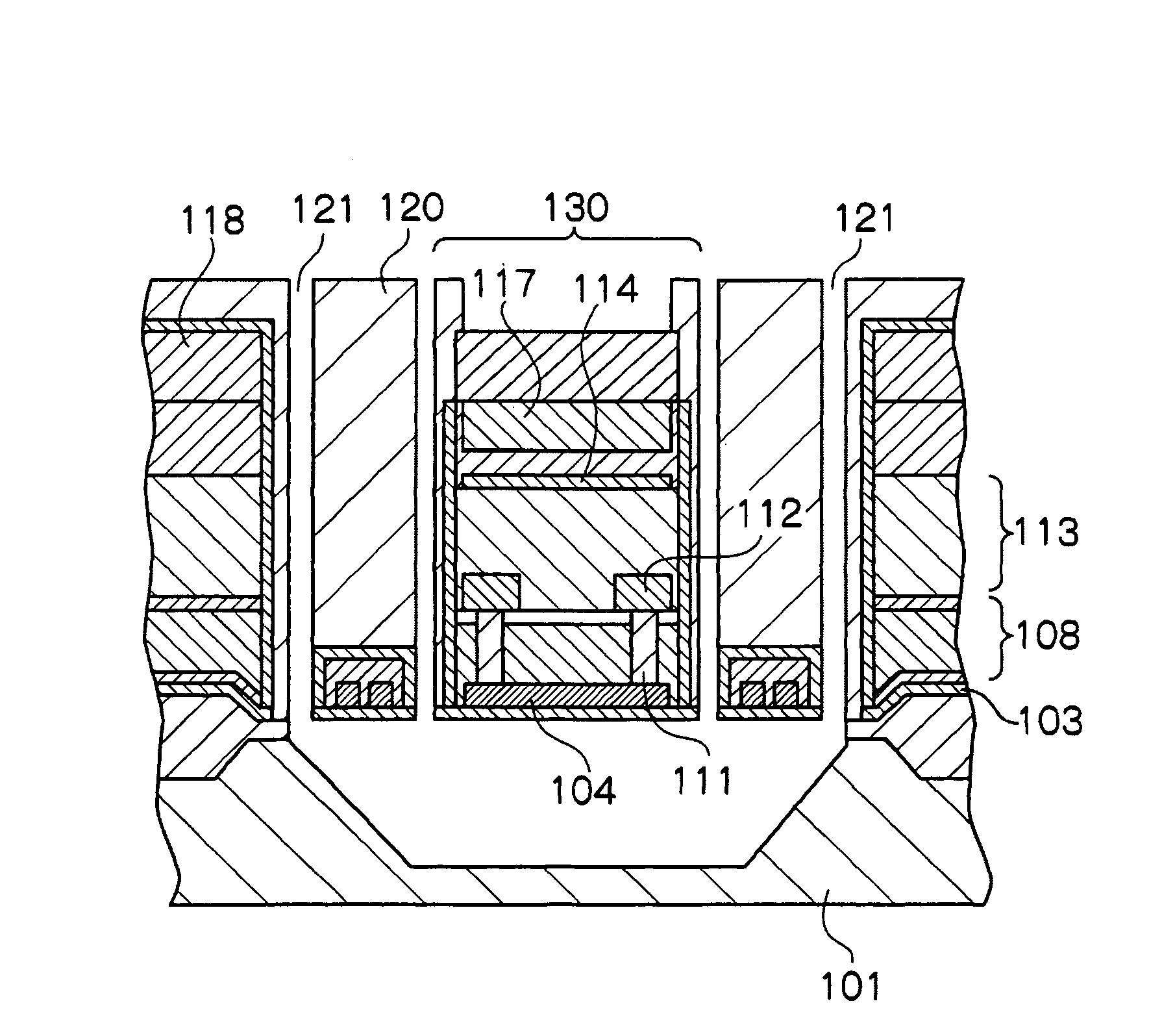
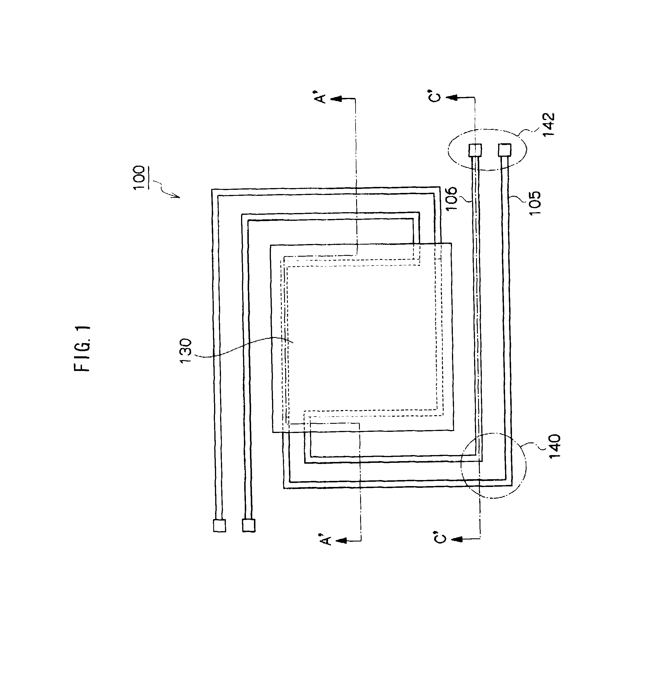
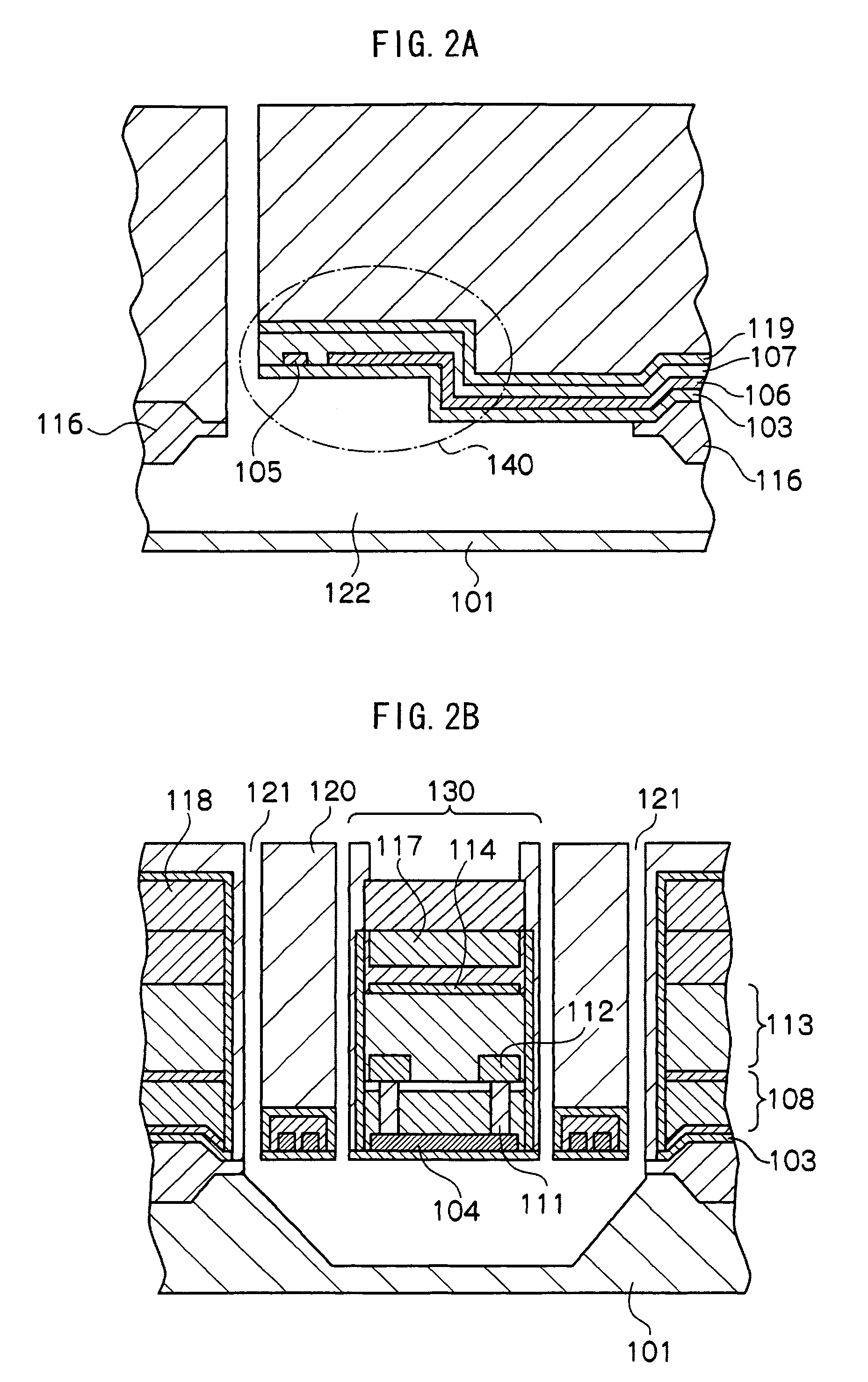
[0073]FIG. 1 is a schematic top view of an infrared detector in a first exemplary embodiment of the invention. FIG. 2A is a C-C′ sectional view of FIG. 1 of an infrared detector in the first exemplary embodiment of the invention. FIG. 2B is an A-A′ sectional view in FIG. 1 of the infrared detector of the first exemplary embodiment of the invention.

[0074]In an infrared detector 100 in the first exemplary embodiment of the invention, a concave portion is formed in a silicon substrate 101 to dispose a void 122. The void 122 is formed by wet etching the silicon substrate 101, and, as shown in FIG. 2B, a sectional shape thereof is, for instance, a trapezoid and, since a (100) plane is etched, an inclined plane becomes a (111) plane. Above the void 122, an infrared receiver 130 is located and the infrared receiver 130 is supported by a beam located above the concave portion and connected to the infrared receiver 130 and a sidewall portion of the silicon substrate 101. A...

second exemplary embodiment

[0088]As an infrared detector in the second exemplary embodiment of the invention is an exemplary embodiment where, as shown in FIG. 4, when a beam is extracted from an infrared receiver 230, the beam is extracted from a position set higher by a strain amount.

[0089]Usually, when external impulse is applied, as shown in FIG. 3, a bent portion 140 is most bendable. However, an infrared detector 200 shown in FIG. 4, also to generation of bending due to the self-weight of other than the bent portion or the stress, is preferred in a point that the bent portion does not come into contact with a silicon substrate.

Fabricating Method of Infrared Detector in First Exemplary Embodiment of the Invention

[0090]A fabricating method of an infrared detector in a first exemplary embodiment of the invention includes a step of forming a first polysilicon layer having a step on a silicon substrate, a step of forming an insulating film on the first polysilicon layer, a step of forming a second polysilico...

third exemplary embodiment

[0101]FIG. 11A is a schematic top view of a conventional infrared detector. FIG. 11B is a partial schematic top view of the conventional infrared detector. FIG. 11C is a partial schematic top view of an infrared detector of a third exemplary embodiment of the invention, and FIG. 11D is a partial schematic top view of a modified example of an infrared detector in a third exemplary embodiment of the invention.

[0102]The infrared detector in the third exemplary embodiment of the invention is characterized in that, in FIG. 11A, in a bent portion 740 where a beam is most bendable, a convex shape in a top view such as shown in FIG. 11C is formed. By thus characterizing, in comparison with a shape of FIG. 11B, when a beam is bent, a direction of external stress is altered to enable to suppress a strain amount of the beam from increasing. The convex shape in a top view is preferably disposed to at least one of bent portions of the beam. Furthermore, as a more preferable exemplary embodiment,...


PUM


Abstract

There is provided an infrared detector including: a silicon substrate provided with a concave portion; an infrared receiver having a polysilicon layer; and a beam that supports the infrared receiver above the concave portion, and extends along a side of the infrared receiver from the infrared receiver to connect with the silicon substrate, the beam having at least two bent portions, wherein at least one of the bent portions of the beam is disposed at a position on a side opposite to the concave portion with the polysilicon layer as a reference point.

Description

CROSS-REFERENCE TO RELATED APPLICATION[0001]This application claims priority under 35 USC 119 from Japanese Patent Application No. 2008-011802, the disclosure of which is incorporated by reference herein.BACKGROUND OF THE INVENTION[0002]1. Field of the Invention[0003]The present invention relates to an infrared detector and a fabricating method thereof, in particular, an infrared detector that detects a temperature of an infrared receiver with a thermopile and a fabricating method of the infrared detector.[0004]2. Description of the Related Art[0005]Infrared ray is a collective term for an electromagnetic wave having a wavelength substantially from 0.72 to 1000 μm. It is categorized largely into a short wavelength band (3 to 5 μm) and a long wavelength band (8 to 14 μm). An infrared sensor is divided, from the viewpoint of the operation principle, into a quantum type and a thermal type. The quantum type makes use of series excitation of sensor elements due to photons of infrared ray...

Claims


Application Information

Patent Timeline
Patent Type & Authority Patents(United States)
IPC IPC(8): H01L31/058
CPCG01J5/02G01J5/023G01J5/20
Inventor ABE, KAZUHIDE
Owner LAPIS SEMICON CO LTD
Why Eureka
Try Eureka