Electronic component package

Inactive Publication Date: 2007-10-18
FUJITSU LTD
View PDF4 Cites 22 Cited by
  • Summary
  • Abstract
  • Description
  • Claims
  • Application Information

AI Technical Summary

Benefits of technology

[0014]Accordingly, the present invention may provide a novel and useful elec

Problems solved by technology

Such an impedance mismatch causes large transmission loss when the si

Method used


Image

  • Electronic component package
  • Electronic component package
  • Electronic component package

Examples


first embodiment

of the Present Invention

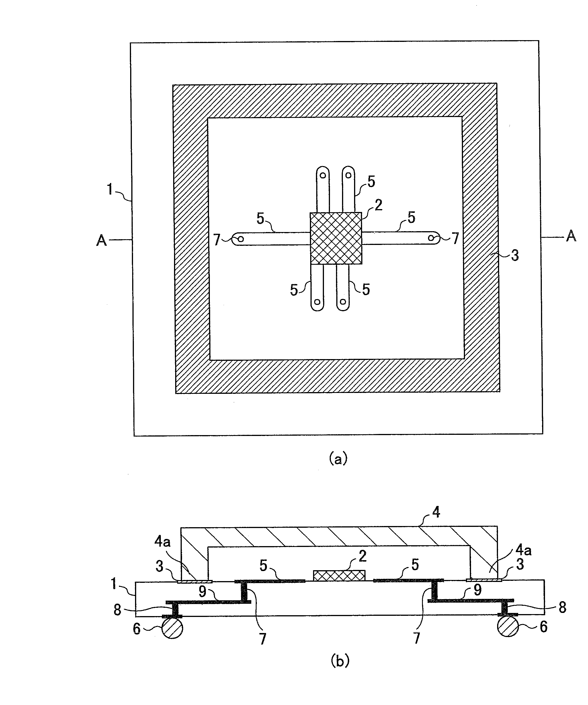
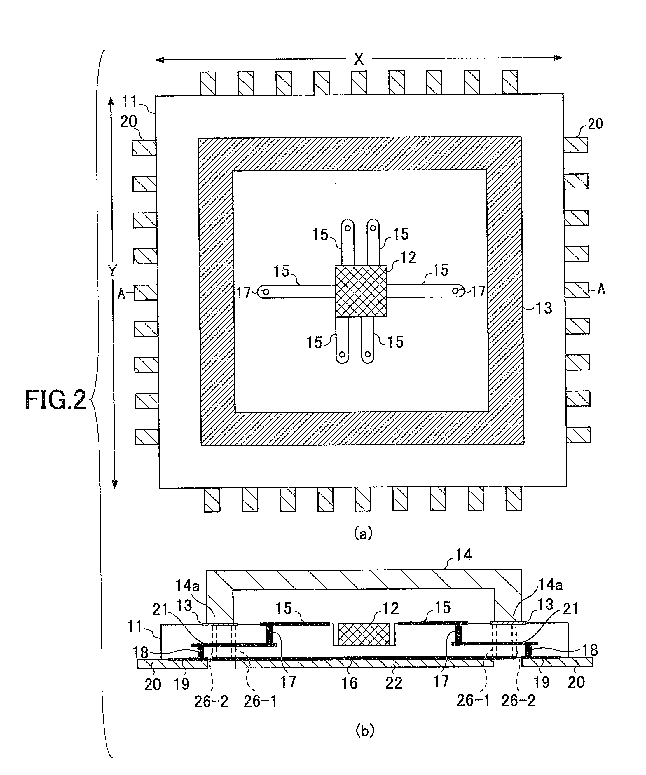
[0055]FIG. 2 is a view showing a schematic structure of a package having an electronic component of a first embodiment of the present invention. More specifically, FIG. 2-(a) is a plan view of a package substrate where a lid part is not provided on an upper surface (first surface). FIG. 2-(b) is a cross-sectional view taken along a line A-A of FIG. 2-(a) where he lid part is provided on the upper surface.

[0056]Referring to FIG. 2, a large scale integrated circuit (LSI) 12 is mounted on a substantially center part of the package substrate 11. A ground conductor 13 made of a metal pattern is provided outside of the LSI 12 along four sides of the upper surface of the package substrate 11 in a substantially rectangular shape.

[0057]The package substrate 1 is a dielectric substrate and may be made of ceramic or the like. While the LSI 12 is illustrated in FIG. 2, the present invention is not limited to this example. An integrated circuit (IC), a passive element, an...

second embodiment

of the Present Invention

[0122]In the above-discussed first embodiment of the present invention, the package substrate 11 has a structure where three signal lines 15, 19 and 21 are alternately provided in the thickness direction. However, the present invention is not limited to this example. The present invention can be applied to a three-layer structure where four signal lines are alternately provided in the thickness direction as an example of a multi-layer structure.

[0123]Here, FIG. 19 is a plan view showing a part of a package substrate having the three-layer structure of a second embodiment of the present invention. FIG. 20 is a cross-sectional view taken along line G-G of FIG. 19. FIG. 21 is a three dimensional view of the three layer structure of the package substrate. FIG. 22 is a cross-sectional view taken along a line H-H of FIG. 19. In FIG. 19 through FIG. 22, parts that are the same as the parts discussed above are given the same reference numerals, and explanation thereo...

third embodiment

of the Present Invention

[0138]In the above-discussed first and second embodiments of the present invention, the lid part 14 provided on the upper surface of the package substrate 11 or 71 has the cross-section of a rectangular shape without one side (inverted “U” shape). However, a part where the lid part and the package substrate 11 come in contact with each other may have a configuration shown in FIG. 23 through FIG. 25, so that a lid part 14 having a plate shape may be mounted on a package substrate 11.

[0139]Here, FIG. 23 is a view showing a schematic structure of a package having an electronic component of a third embodiment of the present invention. FIG. 24 is a detail view of a part surrounded by a dotted line J in FIG. 23. FIG. 25 is a view of a modification of the example shown in FIG. 24. In FIG. 23 through FIG. 25, parts that are the same as the parts discussed above are given the same reference numerals, and explanation thereof is omitted. For the convenience of explanati...


PUM


Abstract

An electronic component package includes a dielectric substrate having a first surface where an electronic component is sealed. A first signal line connecting to the electronic component and a first ground conductor are formed on the first surface of the dielectric substrate. A second signal line connected to an outside connection electrode and a second ground conductor are formed on a second surface of the dielectric substrate. The first ground conductor and the second ground conductor are connected by a plurality of ground conductor via-holes. A substrate-buried signal line connected to the first signal line and the second signal line is provided inside of the dielectric substrate so as to be put between the first ground conductor and the second ground conductor above and below and between the ground conductor via-holes on the right and left.

Description

BACKGROUND OF THE INVENTION[0001]1. Field of the Invention[0002]The present invention generally relates to electronic component packages, and more specifically, to a structure of a package for surface mounting an electronic component used for high speed signal transmission.[0003]2. Description of the Related Art[0004]Conventionally, a sealing package for surface mounting has been widely used as a high speed IC package in an optical communication system or a communication system having an electrooptical interface circuit for signal transmission whose transmission speed is approximately 40 Gbps.[0005]In such a sealing package for surface mounting, an electronic component is sealed in a cavity formed by a dielectric substrate, a lid connected to a surface of the dielectric substrate, and others. The electric component is connected to an electrode formed on a surface of the dielectric substrate opposite to a surface where signal lines are formed.[0006]FIG. 1 is a view showing a related ...

Claims


Application Information

Patent Timeline
IPC IPC(8): H01L23/12
CPCH01L23/10H01L23/13H01L2924/01068H01L2924/01019H01L23/49822H01L23/49838H01L23/50H01L23/66H01L2223/6616H01L2224/16H01L2224/49175H01L2924/01078H01L2924/01079H01L2924/14H01L2924/15153H01L2924/15165H01L2924/15174H01L2924/15311H01L2924/16152H01L2924/1617H01L2924/19051H01L2924/3011H01L24/48H01L24/49H01L2224/48227H01L2924/00H01L2224/05568H01L2224/05573H01L2924/00014H01L2924/30111H01L2224/45099H01L2224/45015H01L2924/207
Inventor CHEUNG, TSZSHINGIKEUCHI, TADASHIYAGISAWA, TAKATOSHI
Owner FUJITSU LTD
Why Eureka
Try Eureka