Liquid crystal display device

a liquid crystal display and display device technology, applied in non-linear optics, instruments, optics, etc., can solve the problems of reducing the performance of moving image display for use with liquid crystal televisions or other devices, reducing and difficulty in increasing the performance of moving image display to a further degree, so as to achieve the effect of higher response characteristics

Active Publication Date: 2007-10-18
PANASONIC LIQUID CRYSTAL DISPLAY CO LTD +1
View PDF14 Cites 53 Cited by
  • Summary
  • Abstract
  • Description
  • Claims
  • Application Information

AI Technical Summary

Benefits of technology

[0014]An object of the invention is to provide a technology that enables an I

Problems solved by technology

The issue here is that an IPS-mode liquid crystal display device has a problem of longer response time compared with a VA-mode liquid crystal display device.
This, problematically, reduces the performance of moving image display for use for a liquid crystal television or others.
However, such a method of reducing the viscosity of a liquid crystal material or narrowing a cell gap has limitations, and has

Method used


Image

  • Liquid crystal display device
  • Liquid crystal display device
  • Liquid crystal display device

Examples


first example

[0068]FIGS. 1 to 7 are each a schematic diagram showing the overall configuration of a liquid crystal display panel for use in a liquid crystal display device in a first example of the invention.

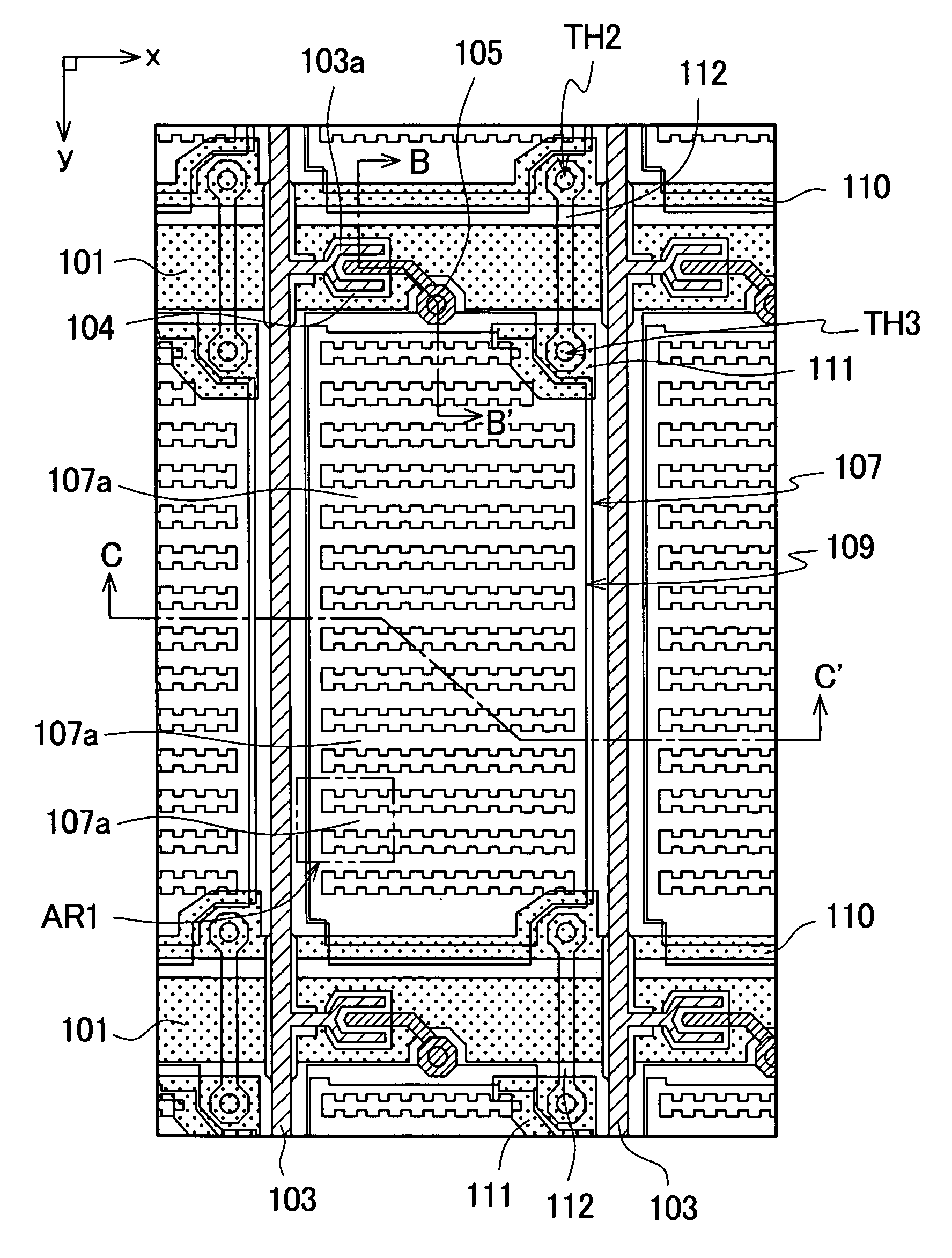
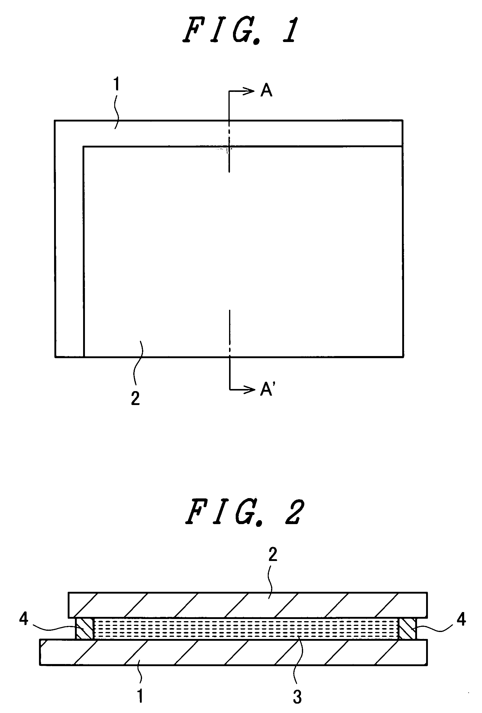
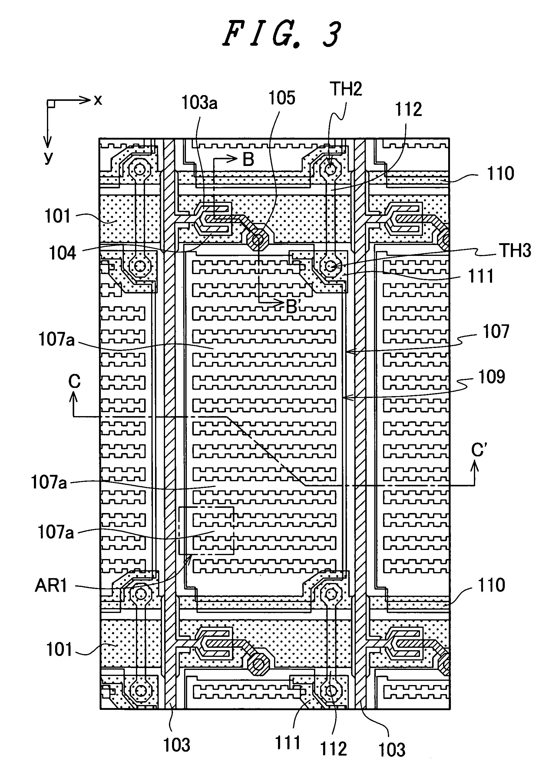
[0069]FIG. 1 is a schematic plan view of the liquid crystal display panel, showing the overall configuration thereof. FIG. 2 is a schematic cross sectional view cut along a line A-A′ of FIG. 1. FIG. 3 is a schematic plan view of a TFT (Thin Film Transistor) substrate of a liquid crystal display panel in a first example, showing an exemplary pixel configuration therein. FIG. 4 is a schematic cross sectional view cut along a line B-B′ of FIG. 3. FIG. 5 is a schematic cross sectional view cut along a line C-C′ of FIG. 3. FIG. 6 is a schematic plan view of a pixel electrode in an area AR1 of FIG. 3, showing an exemplary configuration thereof. FIG. 7 is a schematic plan view of the pixel electrode in the area AR1 of FIG. 3, showing the actual configuration thereof.

[0070]As shown in FIGS. 1 and 2,...

second example

[0141]FIGS. 18 and 19 are each a schematic plan view of a pixel electrode of a liquid crystal display device in a second example, showing the overall configuration thereof. FIG. 18 is a schematic plan view of the pixel electrode in the liquid crystal display device in the second example, showing the overall configuration thereof. FIG. 19 is a schematic plan view of a pixel electrode in an area AR5 of FIG. 18, showing an exemplary configuration thereof.

[0142]In the pixel electrode 107 in the liquid crystal display device of the first example, the comb-like electrode sections 107a are extended in the direction along which the scanning signal lines 101 are extended, i.e., x direction, and are aligned in the direction along which the video signal lines 103 are extended, i.e., y direction. The issue here is that, in the pixel electrode 107 having the comb-like electrode sections 107a, the comb-like electrode sections 107a are not necessarily extended in the x direction, and may be extend...


PUM


Abstract

A liquid crystal display device that includes: a liquid crystal display panel configured by a pair of substrates sandwiching therebetween a liquid crystal material with a positive dielectric anisotropy; and a flat-shaped common electrode and a pixel electrode disposed on one of the pair of substrates with an overlay, via an insulator layer, between the common electrode and the pixel electrode when viewed from above. In the liquid crystal display device, the pixel electrode is extended in a first direction, and includes a plurality of comb-like electrode sections aligned in a second direction orthogonal to the first direction, and the comb-like electrode sections of the pixel electrode are varied in width in the second direction for a plurality of times at intervals shorter than a side extending in the first direction.

Description

[0001]The present application claims priority from Japanese applications JP2006-109990 filed on Apr. 12, 2006, the content of which is hereby incorporated by reference into this application.BACKGROUND OF THE INVENTION[0002]The present invention relates to a liquid crystal display device and, more specifically, to a technology that works well with a liquid crystal display device in which a substrate sandwiching a liquid crystal material with another substrate carries thereon a common electrode and a pixel electrode, and the pixel electrode is disposed above the common electrode via an insulator layer, and includes a comb-like electrode section.[0003]The liquid crystal display device falls into two broad categories of VA (Vertical Alignment) and IPS (In-plane Switching) in view of the direction of an electric field for application to a liquid crystal material, i.e., liquid crystal layer.[0004]In a VA-mode liquid crystal display device, on a substrate sandwiching a liquid crystal mater...

Claims


Application Information

Patent Timeline
IPC IPC(8): G02F1/1343
CPCG02F2201/122G02F1/134363
Inventor SHIMURA, MASATOSASAKI, TOHRUASAKURA, TOSHIKIIMABAYASHI, MAKIKO
Owner PANASONIC LIQUID CRYSTAL DISPLAY CO LTD
Why Eureka
Try Eureka