Circuit Apparatus and Method of Fabricating the Apparatus

Active Publication Date: 2007-11-01
SEMICON COMPONENTS IND LLC +1
3 Cites 21 Cited by

AI-Extracted Technical Summary

Problems solved by technology

If the intimacy of contact in the above-mentioned location is improper, the semiconductor apparatus (circui...

Benefits of technology

[0010] In this background, a general purpose of the present invention is to reduce the likelihood of exfoliat...

Abstract

The likelihood of exfoliation of a sealing resin layer at a pad electrode part is reduced so that the reliability of a circuit apparatus is improved. A circuit apparatus includes a wiring layer, a gold plating layer, an insulating resin layer, a circuit element, a conductive member and sealing resin layer. The gold plating layer is formed in an wiring layer area for the pad electrode. The surface outside the area is roughened. The insulating resin layer is formed so as to cover the wiring layer and to have an opening in an area in which the pad electrode is formed. The circuit element is mounted on a predetermined area on the insulating resin layer. The sealing resin layer is formed on the insulating resin layer so as to entirely cover the circuit element and the opening for the pad electrode. The sealing resin layer, in the area for the pad electrode, is in contact with the gold plating layer and the wiring layer.

Application Domain

Technology Topic

Image

  • Circuit Apparatus and Method of Fabricating the Apparatus
  • Circuit Apparatus and Method of Fabricating the Apparatus
  • Circuit Apparatus and Method of Fabricating the Apparatus

Examples

  • Experimental program(5)

Example

First Embodiment
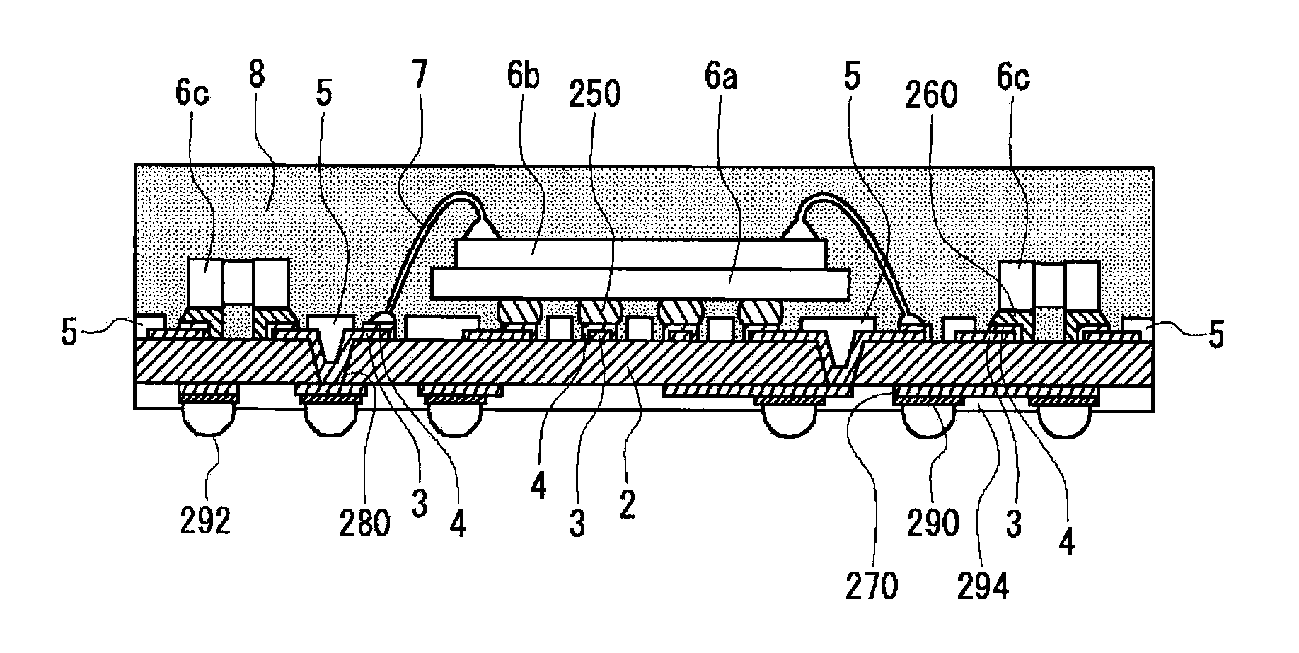
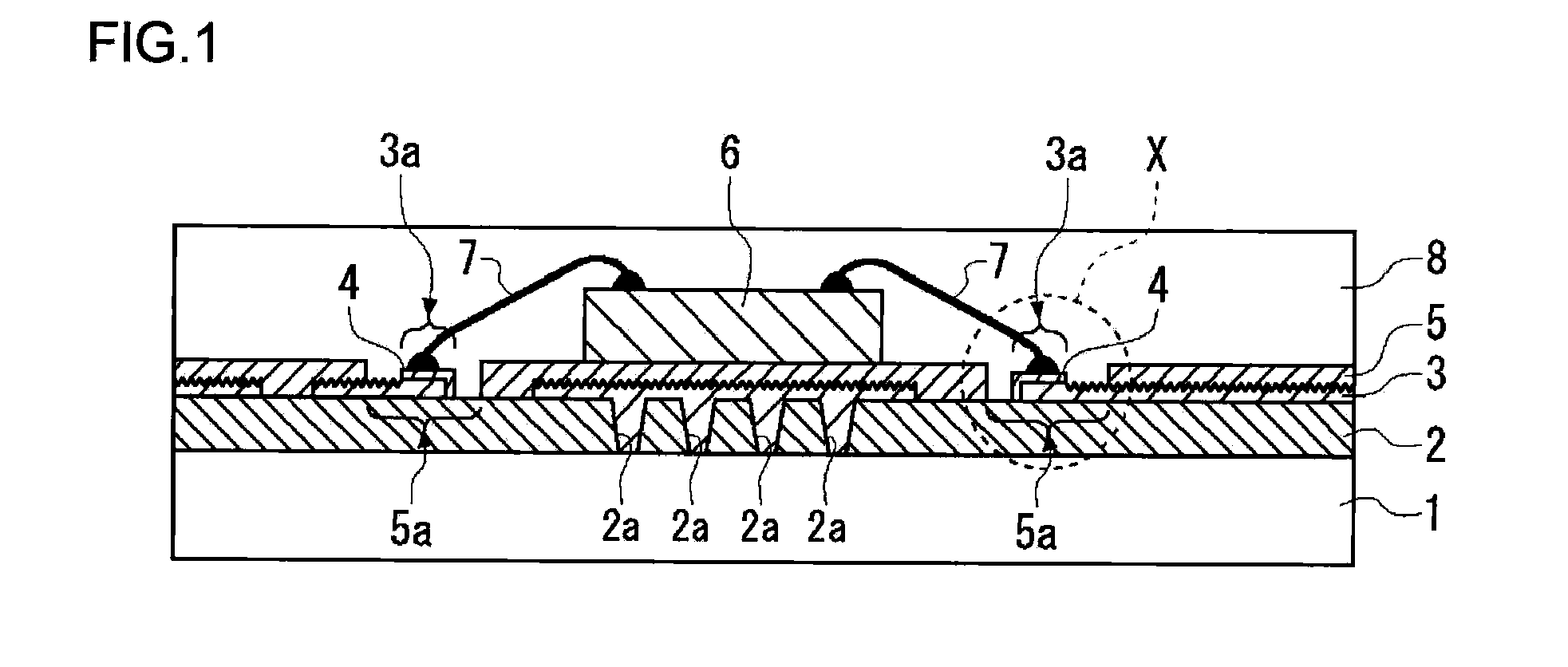
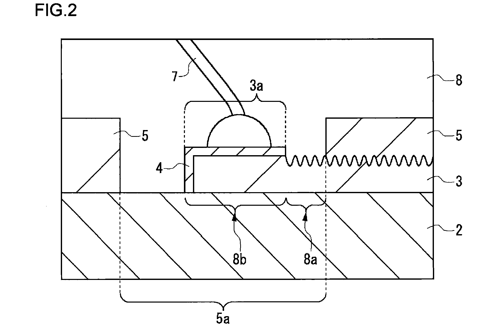
[0048]FIG. 1 is a schematic sectional view of a circuit apparatus according to a first embodiment provided with a pad electrode. FIG. 2 is a sectional view showing a pad electrode part (cross section indicated by X in FIG. 1) of the circuit apparatus shown in FIG. 1 on an enlarged scale. A description will be given of the circuit apparatus according to the first embodiment with reference to FIGS. 1 and 2.
[0049] The circuit apparatus according to the first embodiment is provided with a metal substrate 1, an insulating layer 2, a wiring layer 3 (pad electrode 3a), a gold plating layer 4, an insulating resin layer 5, a circuit element 6, a conductive member 7 and a sealing resin layer 8.
[0050] The metal substrate 1 is implemented by, for example, a copper (Cu) substrate having a thickness of about 1.5 mm. The assembly comprising the metal substrate 1 and the insulating layer 2 is an example of the “substrate” according to the invention.
[0051] A film primarily composed of epoxy resin is employed to form the insulating layer 2. The thickness of the layer 2 is about, for example, 80 μm. It is preferable that the insulating layer 2 be highly heat conductive for improvement in heat dissipation from the circuit apparatus. For this purpose, the insulating layer 2 preferably includes a highly heat conductive filler of, for example, silver, bismuth, copper, aluminum, magnesium, tin, zinc or an alloy thereof. The filler may alternatively comprise silica, alumina, silicon nitride or aluminum nitride.
[0052] In the first embodiment, four via holes 2a having a diameter of about 70 μm and running through the insulating layer 2 in the direction of thickness are formed at predetermined intervals in an area in the insulating layer 2 located below the circuit element 6 described later. A member constituting the wiring layer 3 mentioned later is embedded in each of the via holes 2a. The wiring layer 3 is in contact with the top surface of the metal substrate 1 via the via holes 2a. The wiring layer 3 embedded in the via hole 2a has the function of conducting heat from the circuit element 6 to the metal substrate 1 and dissipating the heat.
[0053] A metal such as copper or aluminum is employed to form the wiring layer 3. The thickness of the layer 3 is about, for example, 20 μm. The wiring layer 3 includes a pad electrode 3a in a portion thereof and is worked to present a predetermined wiring pattern. A gold plating layer 4 is formed on the surface of the pad electrode 3a of the wiring layer 3. The surface of the wiring layer 3 outside the pad electrode 3a is roughened. The arithmetic average roughness Ra of the wiring layer 3 with the roughened surface is preferably about 0.2 μm-10 μm. A copper wiring with the roughness Ra of about 0.38 μm as a result of the roughening process is employed in the illustrated example. The roughness Ra of the copper wiring prior to the roughening process is about 0.25 μm.
[0054] A plating film of electrolytic Au/Ni is used to form the gold plating layer 4. The thickness of the layer is about, for example, 0.5 μm. The gold plating layer 4 is formed to cover a portion of the surface of the wiring layer 3 where the pad electrode 3a is formed. The pad electrode 3a is an example of the electrode of the present invention. The roughness Ra of the gold plating layer 4 is about 0.11 μm. The roughness (arithmetic average roughness Ra) of the surface of the gold plating 4 is smaller than that of the surface of the wiring layer 3 formed of copper, resulting in smaller anchor effect between the layer 4 and the sealing resin layer 8. Therefore, the gold plating layer 4 provides less intimate contact than the copper wiring layer 3.
[0055] A solder resist film comprising epoxy resin is employed to form the insulating resin layer 5. The thickness of the layer 5 is about, for example, 30 μm. The insulating resin layer 5 is formed on the assembly comprising the insulating layer 2 and the wiring layer 3 and is provided with an opening 5a corresponding to the area in the wiring layer 3 that includes the pad electrode 3a. The insulating resin layer 5 functions as a protective film for the wiring layer 3. Since the insulating resin layer 5 is formed on the wiring layer 3, the surface of which is roughened, intimate contact occurs at the interface.
[0056] The circuit element 6 is, for example, a semiconductor element such as an IC chip or an LSI chip, or a passive element such as a capacitor or a resistor. In this case, an LSI chip provided with a pad electrode (not shown) on its top surface is employed. The circuit element 6 is mounted on a predetermined area on the insulating resin layer 5.
[0057] For example, a gold wire is employed to form the conductive member 7 to wire bond between the pad electrode 3a of the wiring layer 3 and the circuit element 6 via the gold plating layer 4 for electrical connection.
[0058] The sealing resin layer 8 is formed so as to entirely cover the insulating resin layer 5, the circuit element 6 and the opening 5a in the insulating resin layer 5. At the opening 5a, the sealing resin layer 8 is in contact with the gold plating layer 4, the insulating layer 2 and the wiring layer 3. The sealing resin layer 8 protects the circuit element 6 from conditions external to the apparatus. For example, thermosetting insulating resin such as epoxy resin is used to form the sealing resin layer 8. A filler for enhancing heat conductivity may be added to the sealing resin layer 8.
[0059]FIG. 3 is an enlarged top view of the pad electrode part (shown in a cross section indicated by X in FIG. 1) of the circuit apparatus shown in FIG. 1. The surface where the sealing resin layer 8 is contact with the wiring layer 3 (area 8a) is located between an area of connection 8b with the conductive member 7 and the wiring pattern covered by the insulating resin layer 5.
[0060] (Method of Fabrication)
First Process for Fabricating the Circuit Apparatus According to the First Embodiment
[0061]FIGS. 4A through 5D are sectional views illustrating the first process for fabricating the circuit apparatus according to the first embodiment shown in FIG. 1. A description will now be given of the first process for fabricating the circuit apparatus according to the first embodiment with reference to FIGS. 1, 4A-4E and 5A-5D.
[0062] As shown in FIG. 4A, a stacked film comprising the insulating layer 2 having a thickness of about 80 μm and a copper foil 3z having a thickness of about 3 μm is pressure bonded to the metal substrate 1.
[0063] As shown in FIG. 4B, photolithography and etching are used to remove the copper foil 3z located where the via holes 2a (see FIG. 1) are formed. In this way, the area in the insulating layer 2 where the via holes 2a are formed is exposed.
[0064] As shown in FIG. 4C, the copper foil 3z is irradiated by CO2 laser or UV laser from above so as to remove an area extending from the exposed surface of the insulating layer 2 to the surface of the metal substrate 1. In this way, the via hole 2a having a diameter of about 70 μm at the surface and running through the insulating layer 2 is formed.
[0065] As shown in FIG. 4D, electroless plating is used to plate the surface of the copper foil 3z and the interior of the via hole 2a with copper to a depth of about 0.5 μm. Subsequently, electroplating is used to plate the surface of the copper foil 8z and the interior of the via hole 7a with copper. In this embodiment, an inhibitor and an accelerator are added to the plating solution, so that the inhibitor is absorbed by the surface of the copper foil 3z and the accelerator is absorbed by the interior of the via hole 2a. This can enlarge the thickness of copper plating in the interior of the via hole 2a. Thereby, the via hole 2a is filled with copper. As a result, as shown in FIG. 4D, the wiring layer 8 having a thickness of about 20 μm is formed on the insulating layer 2 and the via hole 2a is filled by the wiring layer 3.
[0066] As shown in FIG. 4E, photolithography and etching are used to pattern the wiring layer 3. In this way, the wiring layer 3 having a predetermined wiring pattern (pad electrode 3a etc.) is formed.
[0067] Subsequently, as shown in FIG. 5A, selective plating is used to form a gold plating layer (electrolytic Au/Ni plating film) on the surface of a predetermined area (area for the pad electrode 3a) of the wiring layer 3. The area where the gold plating layer 4 is formed is as illustrated in FIG. 3 mentioned earlier.
[0068] As shown in FIG. 5B, the surface of the wiring layer 3 is roughened by, for example, wet treatment. By using an acid-based chemical to treat the surface, the surface is turned into a roughened surface with minute irregularities. In this way, the surface of the wiring layer 3 is roughened with minute irreguralities formed therein. The arithmetic average roughness Ra of the wiring layer 3 with the roughened surface is about 0.38 μm, as mentioned earlier. The surface roughness Ra of the wiring layer 3 can be measured with a surface measuring probe. The wet treatment using an acid-based chemical does not roughen the surface of the gold plating layer 4. The roughness Ra of the gold plating layer 4 is about, for example, 0.11 μm.
[0069] As shown in FIG. 5C, the insulating resin layer 5 is formed so as to cover the insulating layer 2 and the wiring layer 3 and to have an opening 5a corresponding to the area in the wiring layer 3 in which the pad electrode 3a is formed. The thickness of the insulating resin layer 5 is about 30 μm. Since the insulating resin layer 5 is formed on the wiring layer 3, the surface of which is roughened, intimate contact with the insulating resin layer 5 is ensured.
[0070] As shown in FIG. 5D, the circuit element 6 is mounted on the insulating resin layer 5. The circuit element 6 is, for example, an LSI chip provided with a pad electrode (not shown) on its top surface. Subsequently, the conductive member 7 is used to wire-bond the pad electrode of the wiring layer 3 to the circuit element 6 via the gold plating layer 4. This establishes electrical connection between the circuit element 6 and the wiring layer 3.
[0071] Finally, as shown in FIG. 1, the sealing resin layer 8 is formed on the insulating resin layer 5 so as to cover the circuit element 6 and the opening 5a for the pad electrode 3a. In this process, it is ensured that the sealing resin layer 8 covers the pad electrode 3a such that the layer 8 is in contact with both the gold plating layer 4 and the wiring layer 3. As mentioned earlier, the roughness (arithmetic average roughness Ra) of the surface of the copper wiring layer 3 is larger than that of the gold layer 4. As a result, the anchor effect between the layer 3 and the sealing resin layer 8 is more pronounced than between the gold plating layer 4 and the layer 8.
[0072] The circuit apparatus according to the first embodiment is produced through the steps described above.
[0073] The following advantages are provided by the circuit apparatus according to the first embodiment.
[0074] (1) The sealing resin layer 8 at the pad electrode 3a is not only in contact with the gold plating layer 4 but also in contact with the wiring layer 3, which provides more intimate contact than the gold plating layer 4. Thus, the intimacy of contact with the sealing resin layer 8 at the pad electrode 3a is improved as compared with the case where the layer 8 is only in contact with the gold plating layer. Consequently, the circuit apparatus is less affected by thermal stress and humidity, resulting in improved reliability of the apparatus.
[0075] (2) Degradation on the surface of the pad electrode occurring if the wiring layer 3 is formed of copper is minimized since the gold plating layer 4 is provided on the surface of the pad electrode 3a. Therefore, the intimacy of contact between the pad electrode 3a and the sealing resin layer 8 is improved and, further, improper connection between the circuit element 6 and the wiring layer 3 in the circuit apparatus is minimized. As a result, the reliability of the circuit apparatus is further improved.
[0076] (3) Since the surface of the wiring layer 3 in contact with the sealing resin layer 8 is roughened, the intimacy of contact at the interface between the wiring layer 3 and the sealing resin layer 8 is further improved so that the likelihood of exfoliation of the sealing resin layer 8 at the pad electrode 3a is effectively reduced.
Second Process for Fabricating the Circuit Apparatus According to the First Embodiment
[0077] A description will now be given of the second process for fabricating the circuit apparatus according to the first embodiment. A description of those steps that are similar to those of the first fabrication process is omitted as appropriate. The description below highlights those aspects that are different from the corresponding aspects of the first fabrication process. FIGS. 6A-6D and 8A-8B are top views of a pad area, illustrating the second process for fabricating the circuit apparatus according to the first embodiment shown in FIG. 1. FIGS. 7A-7D and 9A-9B are sectional views along A-A′ of FIGS. 6A-6D and 8A-8B, respectively. In FIGS. 7A-9B, the essential part of the pad electrode in the circuit apparatus according to the first embodiment is illustrated.
[0078] The second fabrication process involves the same steps shown in FIGS. 4A-4E illustrating the first fabrication process.
[0079] Subsequent to the step shown in FIG. 4E, as shown in FIGS. 6A and 7A, a conductive layer 100 of flash copper is formed on the insulating layer 2 and the wiring layer 3 by electroless plating. The thickness of the conductive layer 100 is, for example, 1 μm. A circular pad area resembling a tip of a matchstick is formed at the end of the wiring layer 3. The pad area may be rectangular in shape instead of circular.
[0080] Subsequently, as shown in FIG. 6B and 7B, a resist 120 resistant to gold is stacked on the conductive layer 100. An opening R is then formed in the pad area by exposing and developing the resist 120. This exposes the conductive layer 100 at the opening R.
[0081] Subsequently, as shown in FIGS. 6C and 7C, the conductive layer 100 inside the opening R is removed by etching the layer 100 by using a mixture of sulfuric acid and hydrogen peroxide. This results in the wiring layer 3 and the surrounding insulating layer 2 being exposed in the opening R.
[0082] Subsequently, as shown in FIG. 6D and FIG. 7D, the gold plating layer (electrolytic Au/Ni plating film) is formed by electroplating on the wiring layer 3 exposed in the opening R, by using the conductive layer 100 provided beneath the resist 120 as a bus line.
[0083] Subsequently, as shown in FIGS. 8A and 9A, the resist 120 is removed and a mixture of sulfuric acid and hydrogen peroxide is used to remove the conductive layer 100 by etching. Etching also roughens the surface of the wiring layer 3 as explained in the first fabrication process.
[0084] Subsequently, as shown in FIGS. 8B and 9B, the insulating resin layer (photosolder resist) 5 is stacked upon the assembly. An opening R′ is formed in the pad area by exposing and developing the layer 5. The opening R′ is larger than the opening R to ensure that a part of the wiring layer 3 not covered by the gold plating layer 4 is exposed. This ensures that the gold plating layer 4 and the area of the wiring layer 3, which is in adjacent to the gold plating layer 4 and is roughened, are exposed. Since the underside of the insulating resin layer 5 is in contact with the wiring layer 3 which is roughened, intimacy of contact between the wiring layer 3 and the insulating resin layer 5 is improved due to the anchor effect.
[0085] The structure corresponding to that of FIG. 5C of the first fabrication process is obtained through the steps described above. By performing the similar steps as in the first fabrication process subsequently, the circuit apparatus according to the first embodiment is fabricated.
[0086] The following advantages are provided by the circuit apparatus according to the second fabrication process.
[0087] (4) For formation of the gold plating layer 4 in the pad area by selective plating, a bus line for plating connected to the pad area should be formed. Dicing into individual pieces results in the bus line for plating being severed. However, part of the bus line leading from the dicing line to the pad area remains. The remaining bus line may generate noise by operating as an antenna. According to the second fabrication process, however, the conductive layer 100 of flash copper formed on the wiring layer 3 is used as a bus line, and the conductive layer 100 is removed after the gold plating layer 4 is formed. Therefore, it is ensured that the bus line for plating does not represent a source of noise.
[0088] (5) For formation of the gold plating layer 4 in the pad area by selective plating, a bus line for plating connected to the pad area should be formed. This may impose constraints on the layout of wiring etc. and prevent components from being mounted with high density. Whereas, according to the second fabrication process, the conductive layer 100 for plating is removed after the gold plating layer 4 is formed. Accordingly, there are less constraints on the layout of wiring etc, and attempts for high density of components are likely to be successful.

Example

Second Embodiment
[0089]FIG. 10 is a sectional view of a pad electrode part of a circuit apparatus according to a second embodiment of the present invention. FIG. 11 is a top view of the pad electrode part of the circuit apparatus shown in FIG. 10. The circuit apparatus according to the second embodiment differs from that of the first embodiment in that the area 8a where the sealing resin layer 8 is in contact with the wiring layer 3 is provided around the area for connection 8b in contact with the gold plating layer 4. The other aspects of the second embodiment are the same as the corresponding aspects of the first embodiment.
[0090] The following advantage is provided by the circuit apparatus according to the second embodiment.
[0091] (6) Since the gold plating layer 4 is surrounded by the wiring layer 3 which is roughened, the likelihood of exfoliation of the sealing resin layer 8 from the pad electrode 3a is effectively reduced. As a result, the circuit apparatus with improved reliability is provided.

Example

Third Embodiment
[0092]FIG. 12 is a sectional view of a pad electrode part of a circuit apparatus according to a third embodiment of the present invention. FIG. 13 is a top view of the pad electrode part of the circuit apparatus shown in FIG. 12. The circuit apparatus according to the third embodiment differs from that of the first embodiment in that the area 8a where the sealing resin layer 8 is in contact with the wiring layer 3 is provided around the area for connection 8b in contact with the gold plating layer 4 and that the end of the wiring layer 3 covers the insulating layer 2 between the insulating resin layer 5 and the gold plating layer 4. The other aspects of the third embodiment are the same as the corresponding aspects of the first embodiment.
[0093] The following advantage is provided by the circuit apparatus according to the second embodiment.
[0094] (7) Since the gold plating layer 4 is surrounded by the large area of the wiring layer 3 which is roughened, the likelihood of exfoliation of the pad electrode 3a from the sealing resin layer 8 is effectively reduced. As a result, the circuit apparatus with improved reliability is provided.

PUM

PropertyMeasurementUnit
Electrical conductor
Area
Semiconductor properties
tensileMPa
Particle sizePa
strength10

Description & Claims & Application Information

We can also present the details of the Description, Claims and Application information to help users get a comprehensive understanding of the technical details of the patent, such as background art, summary of invention, brief description of drawings, description of embodiments, and other original content. On the other hand, users can also determine the specific scope of protection of the technology through the list of claims; as well as understand the changes in the life cycle of the technology with the presentation of the patent timeline. Login to view more.

Similar technology patents

Removable clip for beverage lid

InactiveUS20060027588A1Reduce likelihoodStampsCapsBiomedical engineeringDisposable cup
Owner:MACKOVIC BASIC MIRIAM +3

Electronic message distribution

Owner:ORACLE OTC SUBSIDIARY

Container having a base and a lid

InactiveUS20160368677A1Reduce likelihoodEnhance barrier propertyClosure capsTobacco devicesTobacco productEngineering
Owner:JT INT SA

Classification and recommendation of technical efficacy words

  • Improve reliability
  • Reduce likelihood

Arc-shaped cutting anastomat

ActiveCN101912284AGood assembly firmnessImprove reliabilitySurgical staplesDistal anastomosisEngineering
Owner:CHANGZHOU JIANRUIBAO MEDICAL DEVICES

Distributed power harvesting systems using DC power sources

ActiveUS20080143188A1Improve reliabilitySafe operating voltageDc network circuit arrangementsBatteries circuit arrangementsTransverterVoltage variation
Owner:SOLAREDGE TECH LTD

Stent delivery device and method

Owner:BOSTON SCI SCIMED INC
Why Eureka
Try Eureka