Optical Device, an Optical System and a Method of Manufacturing a Holographic Optical Element

a technology of optical elements and optical devices, applied in the field of optical devices, optical systems and methods of manufacturing holographic optical elements, can solve the problems of beams, difficult to maintain two, and difficult to achieve, and achieve the effects of greatly reducing digital hologram recording times, high speed, and effective rotation

Inactive Publication Date: 2007-11-08
MUNDAY ROBERT ADAM +2
View PDF1 Cites 8 Cited by
  • Summary
  • Abstract
  • Description
  • Claims
  • Application Information

AI Technical Summary

Benefits of technology

[0040] Ideally beams are displaced to different positions, relative to the optical axis, in order to produce a desired holographic grating. This is one factor that relates the speed of manipulation of the two beams to the speed of exposure. The amount and speed of displacement is typically measured as pixels per second or exposures per second. In this sense the beams can be displaced typically at a rate of 0.2 kHz to 2 kHz and ideally in excess of 5 kHz using certain optical beam deflectors or scanners. Digital hologram recording times are therefore greatly reduced.
[0041] It will be appreciated that the invention, under control of a controller, for example a microprocessor, is capable of producing a pair of superimposed beams. Moreover as the two beams emanate from a common source they are absolutely identical in every respect (including coherence and polarisation). Furthermore the two beams may be manipulated i.e. displaced laterally in both the x-z and y-z planes and can therefore effectively be rotated about the principal optical axis, by an angle (Ø) at very high speeds and with accuracy and precision.
[0042] An acousto-optic modulator (AOM) may be used as a beam deflector. An advantage of an acousto-optic beam deflector is that it can be operated at high frequencies, typically in excess of 5 kHz, and preferably in excess of 10 kHz, thereby enabling holographic production rates to be further increased. An alternative beam deflector utilises a piezoelectric (PZ) element. A further alternative beam deflector is a galvanometric beam deflector and is typically capable of exposing 3000 points per second.

Problems solved by technology

Previously this has been difficult to achieve because it has proven difficult to maintain two, independently focused, beams in true and perfect alignment one with another.

Method used


Image

  • Optical Device, an Optical System and a Method of Manufacturing a Holographic Optical Element
  • Optical Device, an Optical System and a Method of Manufacturing a Holographic Optical Element
  • Optical Device, an Optical System and a Method of Manufacturing a Holographic Optical Element

Examples


Embodiment Construction

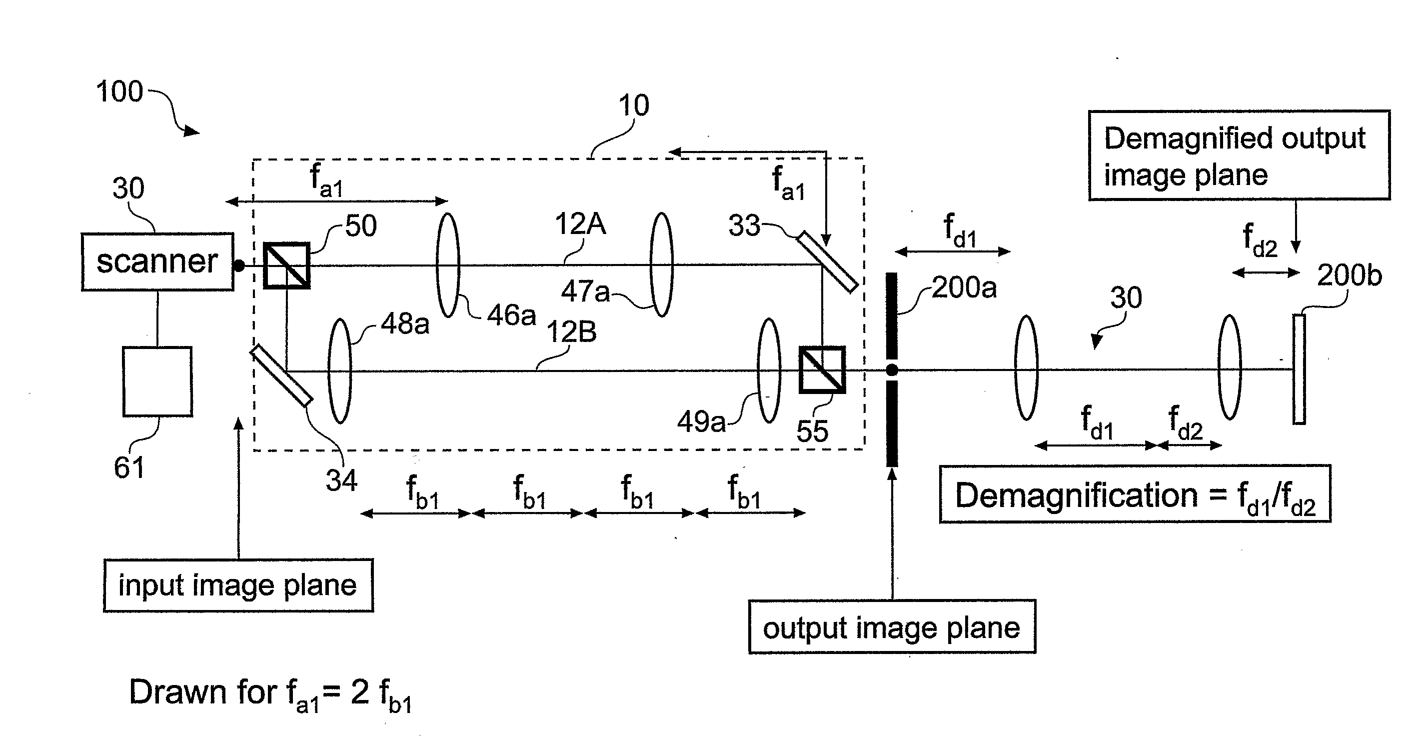
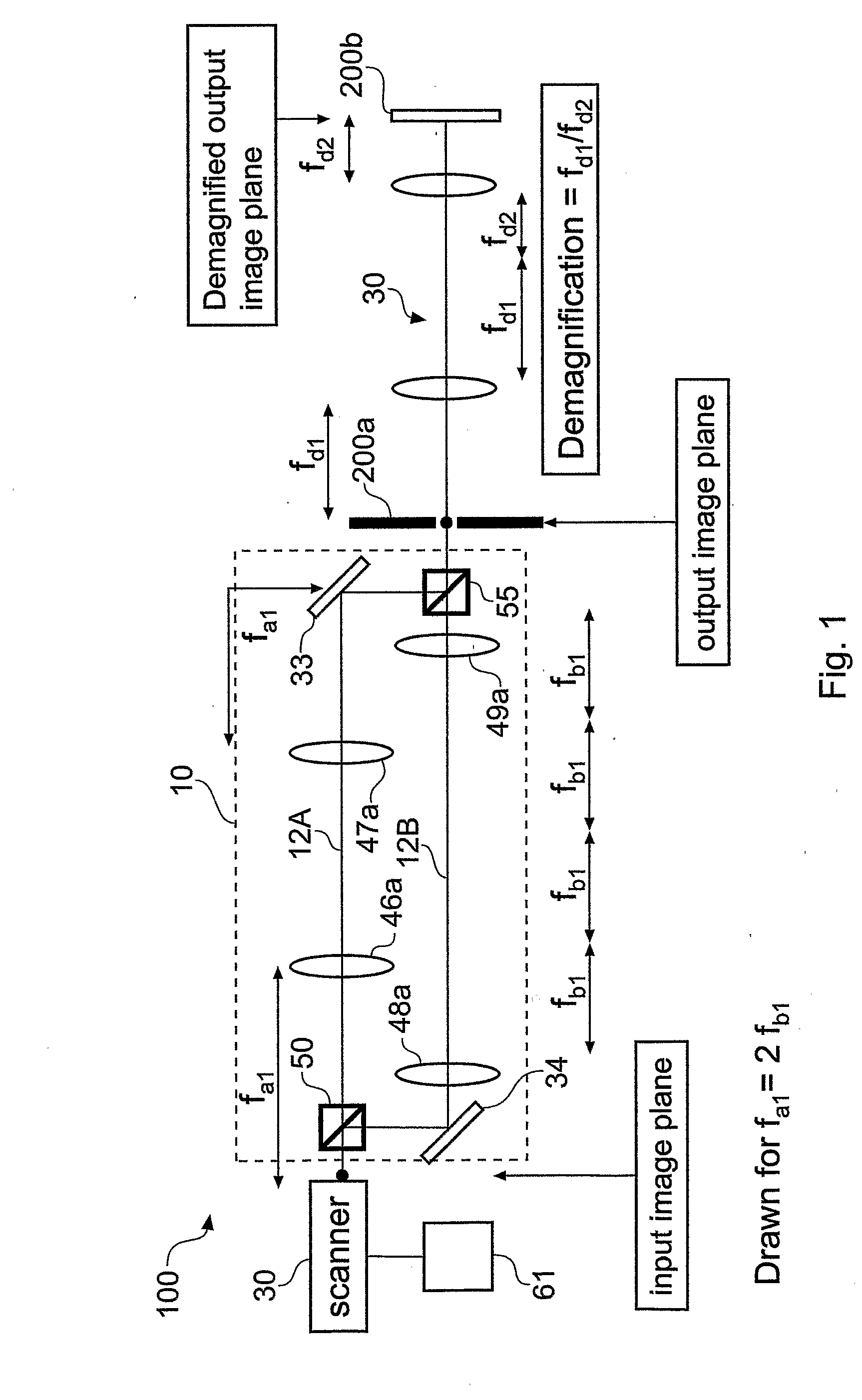
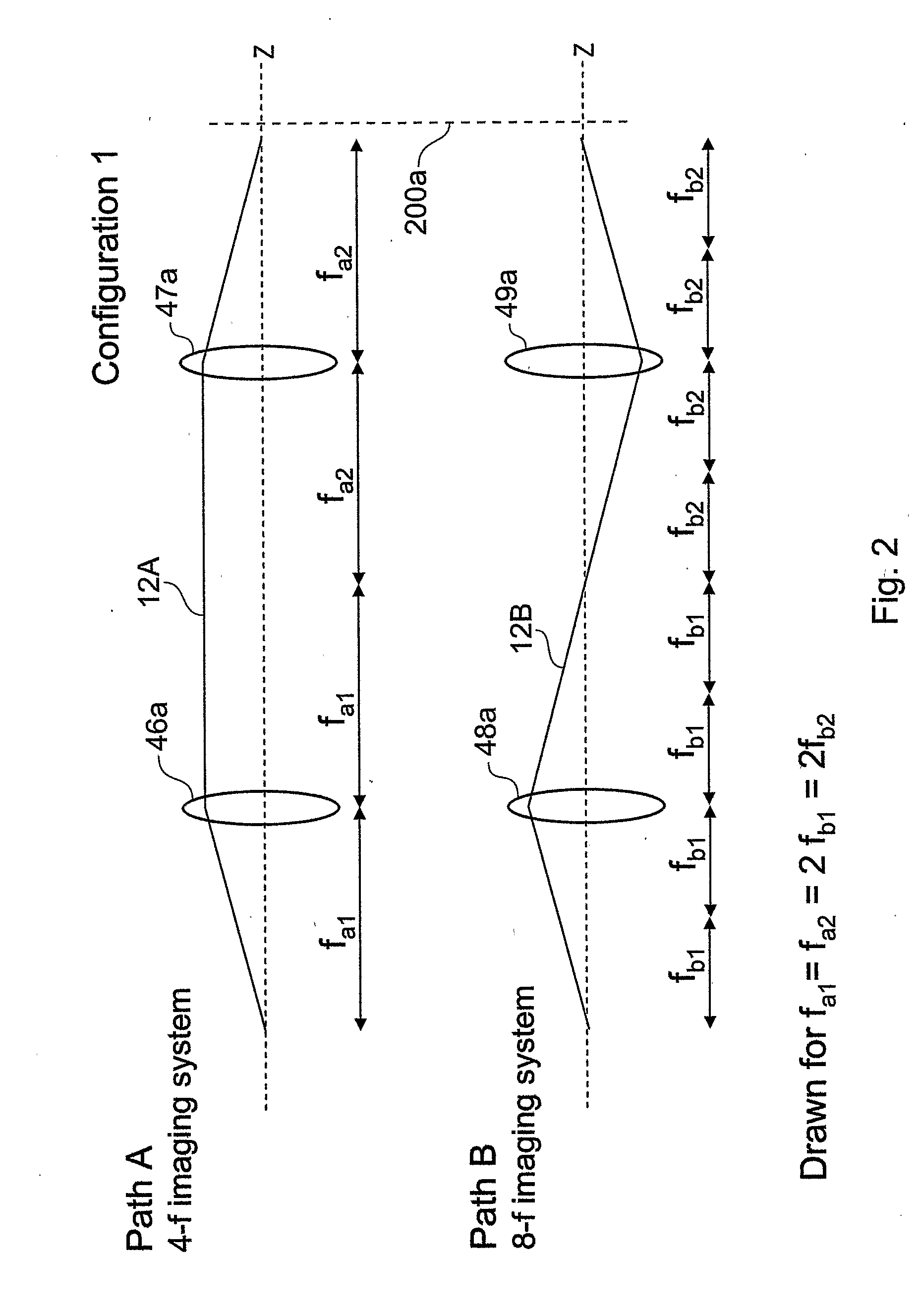
[0061] Referring to the Figures generally, in which like parts bear the same reference numerals, there is shown a device 10 incorporated in an optical system 100 for producing a hologram (not shown) at an output plane 200. The output plane 200 may be located at either of two positions 200a or 200b in dependence upon whether an image reduction device is included.

[0062] The optical system 100 includes a modulated laser 60 for producing a coherent light beam 12 and a scanner 30 for deflecting the light beam 12 in accordance with control signals from a controller. A photoresist coated plate or other holographic supporting medium is located at the output plane 200a or 200b and it is here where the hologram is formed. The photoresist coated plate is typically supported so that relative displacement is achieved between the system and the photoresist coated plate (or other holographic supporting medium), so that pixels can be defined at different locations on the photoresist coated plate. ...


PUM


Abstract

This invention relates to an optical device and system for producing a holographic optical element or digital hologram. Various techniques of producing digital holograms have been proposed. However, they tend to suffer from long exposure times, as well as problems associated with control of two or more independent beams of coherent light used to produce a hologram. Problems become even more acute as pixel size decreases. The present invention provides an optical device including: a beam deflector, adapted to deflect a collimated beam of coherent light to produce an incident beam; a beam splitter for producing first and second beams, said beams being displaced so that the angle of deflection of the first beam is the same but opposite to the angle of deflection of the second beam; and a combiner combines the first and second beams so as to produce an interference pattern at an output plane.

Description

BACKGROUND [0001] This invention relates to an optical device, an optical system and a method of manufacturing a holographic optical element. [0002] More particularly, but not exclusively, the invention relates to a device and system, which is suitable for producing a holographic optical element, holographic micro-lens array, dot matrix hologram or digital hologram. A holographic optical element, holographic micro-lens array or dot matrix hologram is hereinafter referred to as a digital hologram. [0003] Digital holograms have been fabricated since the early 1980's. Typically digital holograms comprise of a plurality of holographic lenses or pixels recorded in an array. Each micro-lens in the array is a small, single, diffractive or refractive, holographic optical element in its own right. [0004] Digital holograms are recorded in the form of a two dimensional array which can have any pattern or layout. Each holographic micro-lens in the array redirects light that is transmitted throu...

Claims


Application Information

Patent Timeline
Patent Type & Authority Applications(United States)
IPC IPC(8): G03H1/30G03H1/04
CPCG03H1/30G03H2001/0296G03H2001/0413G03H2260/63G03H2001/0497G03H2260/62G03H2001/0482
Inventor MUNDAY, ROBERT ADAMFRENCH, PAUL MICHAEL WILLIAMPITAVY, OLLVIER
Owner MUNDAY ROBERT ADAM
Why Eureka
Try Eureka