Optical waveguide device and semiconductor device technical field

a technology of optical waveguide and semiconductor, which is applied in the direction of semiconductor lasers, instruments, optical elements, etc., can solve the problems of affecting the operation of the connection interface, and affecting the appearance of wavelength variation of the gain, so as to achieve the effect of stabilizing the operation and suppressing the influence of reflected light on the connection interfa

Active Publication Date: 2007-11-08
FUJITSU LTD
View PDF13 Cites 17 Cited by
  • Summary
  • Abstract
  • Description
  • Claims
  • Application Information

AI Technical Summary

Benefits of technology

[0027] Accordingly, with the optical waveguide devices and the semiconductor devices of the present invention, there is an advantage that, where an optical waveguide device is produced wherein waveguides different in kind from each other are integrated on the same substrate, only if the position of the connection interface is adjusted, then the influence of reflected light on the connection interface can be suppressed easily and with certainty while characteristics of the optical waveguides are compensated for. As a result, in an optical waveguide device wherein waveguides different in kind from each other are integrated on the same substrate, stabilized operation can be implemented.

Problems solved by technology

At present, an optical communication system has a tendency to become a more advanced and complicated system.
Where two devices (optical waveguides) whose materials or structures are different from each other are connected, reflection occurs on the connection interface without fail, and there is the possibility that the reflected light may cause degradation of characteristics of the devices.
For example, where a semiconductor optical amplifier is integrated, gain ripples are generated due to unintended interference by the reflected light, resulting in appearance of wavelength variation of the gain.
Further, for example, where a laser is integrated, an oscillation state of the laser is destabilized by reflection returning light, and this makes stabilized operation difficult.

Method used


Image

  • Optical waveguide device and semiconductor device technical field
  • Optical waveguide device and semiconductor device technical field
  • Optical waveguide device and semiconductor device technical field

Examples


first embodiment

[0084] First, an optical waveguide device (optical waveguide element) and a semiconductor device (semiconductor element) according to a first embodiment of the present invention are described with reference to FIGS. 1 to 10.

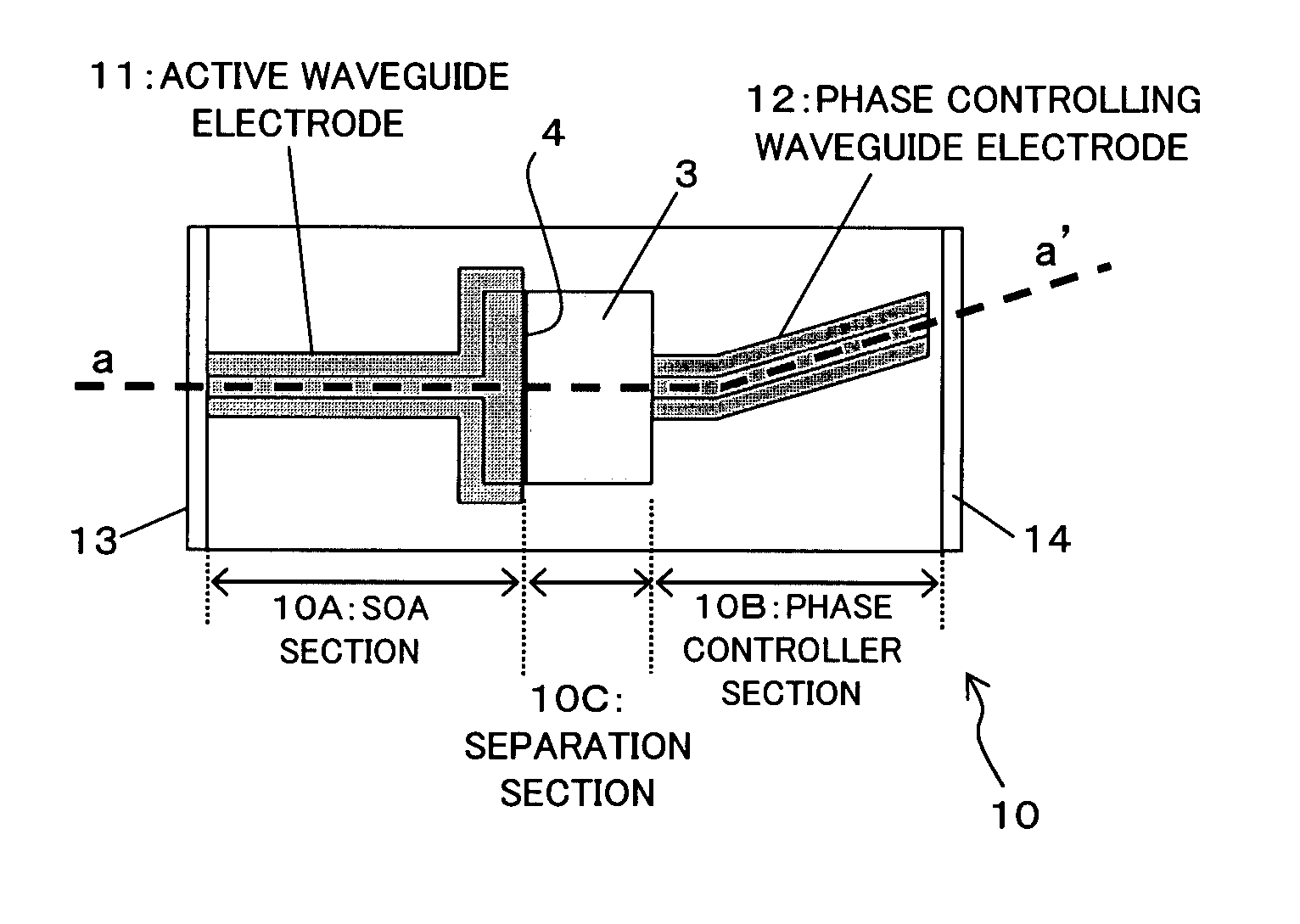
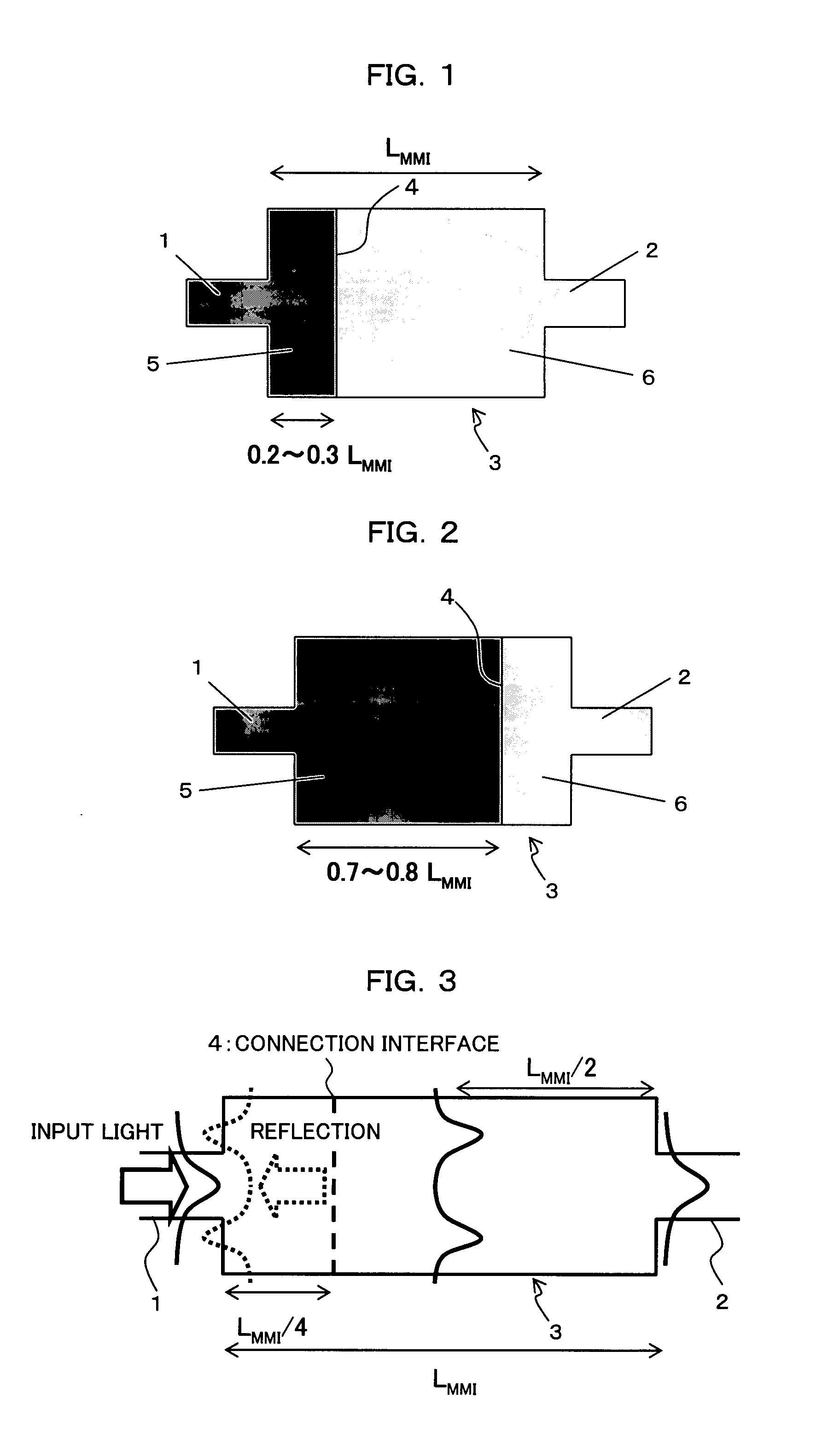
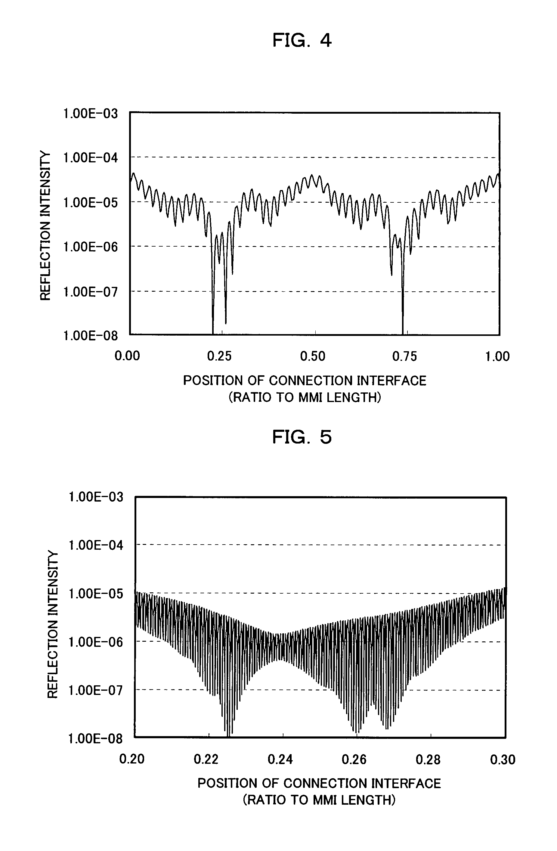
[0085] As shown in FIGS. 1 and 2, the optical waveguide device according to the present embodiment includes at least two kinds of optical waveguides (optical waveguide elements) 1 and 2 formed from materials or in structures different from each other on one substrate, and the optical waveguides 1 and 2 are connected to each other through a 1×1 multimode interference (MMI; MultiMode Interference) waveguide 3. Here, a connection interface (connection plane) 4 between the two kinds of the optical waveguides 1 and 2 is provided so as to be contained in the inside of the 1×1 MMI waveguide 3.

[0086] As shown in FIGS. 1 and 2, the present optical waveguide device includes the first optical waveguide (first single-mode waveguide) 1, the second optical waveguide (second ...

second embodiment

[0165] Next, an optical waveguide device (optical waveguide element) and a semiconductor device (semiconductor element) according to a second embodiment of the present invention are described with reference to FIGS. 11 to 14.

[0166] In the optical waveguide device according to the present embodiment, the positions of the input and output waveguides (that is, positions of the input and output ports) are different from those in the first embodiment described above. In particular, while, in the first embodiment described above, the 1×1 multi-mode interference (MMI) waveguide is configured as a symmetric 1×1 MMI waveguide, in the present embodiment, the 1×1 MMI waveguide is configured as an asymmetric 1×1 MMI waveguide 31 as shown in FIG. 11.

[0167] It is to be noted that the configuration of the other part is same as that in the first embodiment described above. Further, like elements to those in FIG. 11 are denoted by like reference characters to those in the first embodiment (refer t...

third embodiment

[0181] Next, an optical waveguide device (optical waveguide element) and a semiconductor device (semiconductor element) according to the third embodiment of the present invention are described with reference to FIG. 15 (a) to FIG. 19.

[0182] In the optical waveguide device according to the present embodiment, the angles of end faces on the input and output sides of a 1×1 multi-mode interference (MMI) waveguide are different from those of the first and second embodiments described above. In particular, while, in the first and second embodiments described above, the 1×1 MMI waveguide has a rectangular shape as viewed in plan and the end faces on the input and output sides extend perpendicularly to the longitudinal direction (waveguide direction, optical axial direction, optical waveguide direction) of the 1×1 MMI waveguide, in the present embodiment, as shown in FIG. 15(a) to FIG. 15 (c), end faces 7a to 7d on the input and output sides of 1×1 MMI waveguides 3A and 31A extend obliquel...


PUM


Abstract

In order to make it possible to suppress the influence of reflected light on a connection interface easily and with certainty, an optical waveguide device includes a first optical waveguide (1), a second optical waveguide (2) formed from a material or in a structure different from that of the first optical waveguide (1) and connected to the first optical waveguide (1), and a 1×1 multimode interference waveguide (3) formed by increasing the widths of the first optical waveguide (1) and the second optical waveguide (2) in the proximity of a connection interface between the first optical waveguide (1) and the second optical waveguide (2).

Description

TECHNICAL FIELD [0001] The present invention relates to an optical waveguide device and a semiconductor device wherein a plurality of devices are monolithically integrated. BACKGROUND ART [0002] At present, an optical communication system has a tendency to become a more advanced and complicated system. For example, together with higher functionalization of an optical communication system such as a WDM optical communication system, it is demanded to highly functionalize an optical waveguide device (semiconductor device) such as an optical semiconductor device (for example, semiconductor laser or the like) to be used in such an optical communication system as just mentioned. [0003] As one of means for implementing this, it is considered a possible idea to configure an optical waveguide device (optical semiconductor device) as an optical integrated device wherein a plurality of devices are monolithically integrated. [0004] As such an optical integrated device (optical waveguide device)...

Claims


Application Information

Patent Timeline
Patent Type & Authority Applications(United States)
IPC IPC(8): G02B6/26H01S5/12
CPCB82Y20/00H01S5/50G02B6/2813G02B2006/12152G02F1/01708G02F1/025G02F2001/217H01S5/026H01S5/0265H01S5/028H01S5/06206H01S5/101H01S5/1014H01S5/12H01S5/20G02B6/14G02F1/217
Inventor TAKABAYASHI, KAZUMASAMORITO, KEN
Owner FUJITSU LTD
Why Eureka
Try Eureka