

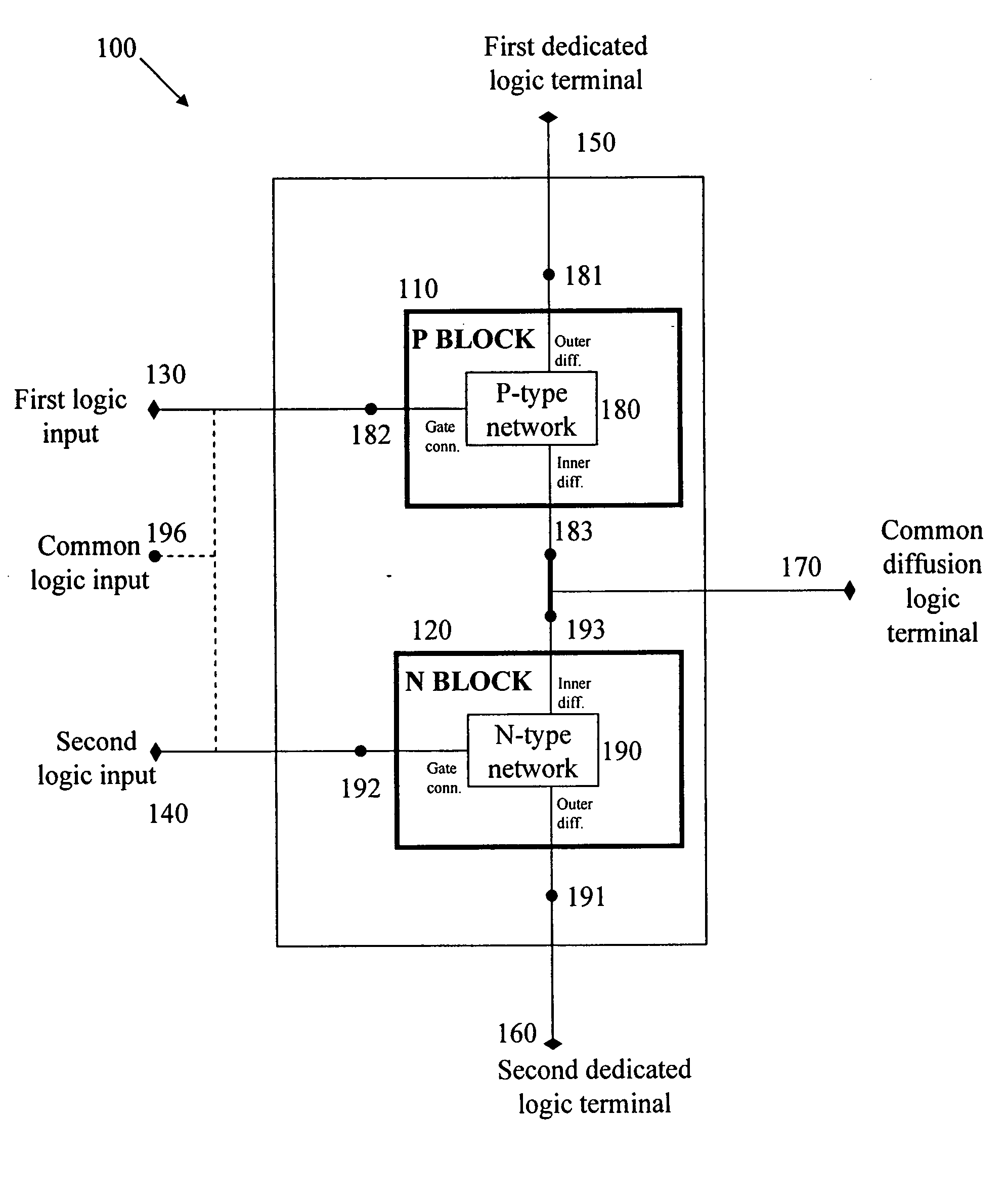
Logic circuit and method of logic circuit design
a logic circuit and logic circuit technology, applied in logic circuits, program control, instruments, etc., can solve the problems of slow operation at reduced supply voltage, reduced current drive, and reduced power requirements of most ptl implementations, so as to reduce the area and power requirements
- Summary
- Abstract
- Description
- Claims
- Application Information
AI Technical Summary
Benefits of technology
Problems solved by technology
Method used
Image

Examples
examples
[0220] Reference is now made to the following examples, which together with the above descriptions illustrate the invention in a non-limiting fashion.
[0221] Simulations were performed to determine the relative performance of five GDI logic gates to other logic gate technologies. Five sets of comparisons were carried out on various logic gates, MUX, OR, AND, F1, and F2. Reference is now made to FIGS. 18a, 18b, and 18c, which show GDI XOR, AND, and OR gates respectively, and their equivalents in CMOS, TG, and NMOS Pass-Gate (N-PG) technologies. The cells were designed for a minimal number of transistors for each technique. A buffer was added to the N-PG cells, because of low swing of output voltage (Vdrop>0.3 VDD). Most circuits were implemented with a W / L ratio of 3, to achieve the best power-delay performance. The logic circuits were designed at the transistor-level in a 0.35 μm twin-well CMOS technology (with VTN=0.56V and VTP=−0.65V). The circuits were simulated using Cadence Spe...
PUM
 Abstract
Description
Claims
Application Information