Al technical title is built by PatSnap Al team. It summarizes the technical point description of the patent document.
a free space and interchip technology, applied in the direction of transit-time tubes, electrical devices, electric discharge tubes, etc., can solve the problems of constrained communication speeds of chips that are electrically connected in this manner
Inactive Publication Date: 2007-11-15
ADVANCED PLASMONICS
View PDF99 Cites 58 Cited by
Summary
Abstract
Description
Claims
Application Information
AI Technical Summary
This helps you quickly interpret patents by identifying the three key elements:
Problems solved by technology
Method used
Benefits of technology
Problems solved by technology
However, chips that are electrically connected in that manner have experienced constrained communication speeds as compared to optical connections.
Method used
Image
Click on the blue label to locate the original text in one second.
Reading with bidirectional positioning of images and text.
Examples
Embodiment Construction
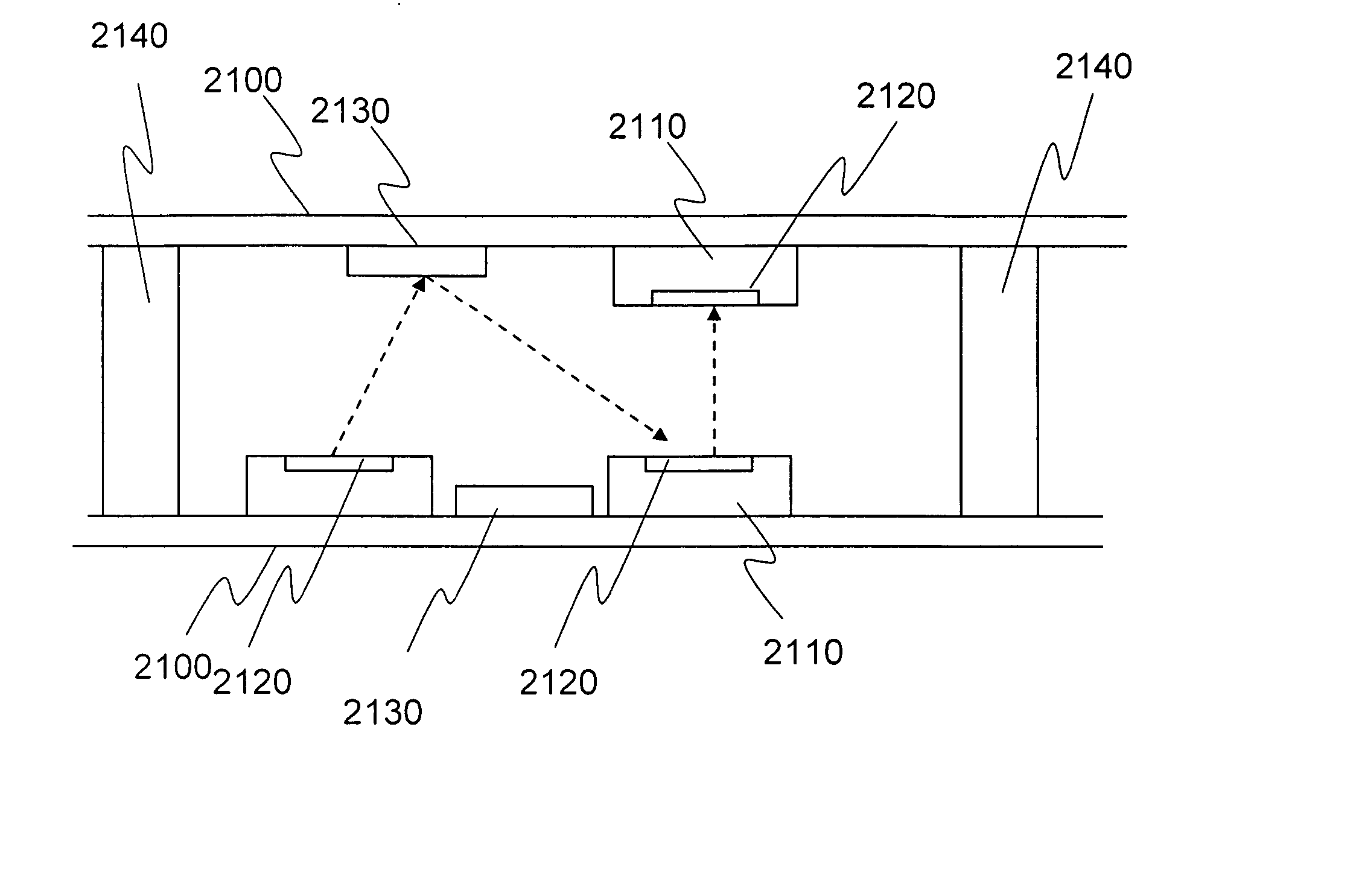
[0039] Turning to FIG. 1, according to the present invention, a wavelength element 100 on a substrate 105 (such as a semiconductor substrate or a circuit board) can be produced from at least one resonant structure 110 that emits light (such as infrared light, visible light or ultraviolet light or any other electromagnetic radiation (EMR) 150 at a wide range of frequencies, and often at a frequency higher than that of microwave). The EMR 150 is emitted when the resonant structure 110 is exposed to a beam 130 of charged particles ejected from or emitted by a source of charged particles 140. The source 140 is controlled by applying a signal on data input 145. The source 140 can be any desired source of charged particles such as an electron gun, a cathode, an ion source, an electron source from a scanning electron microscope, etc.
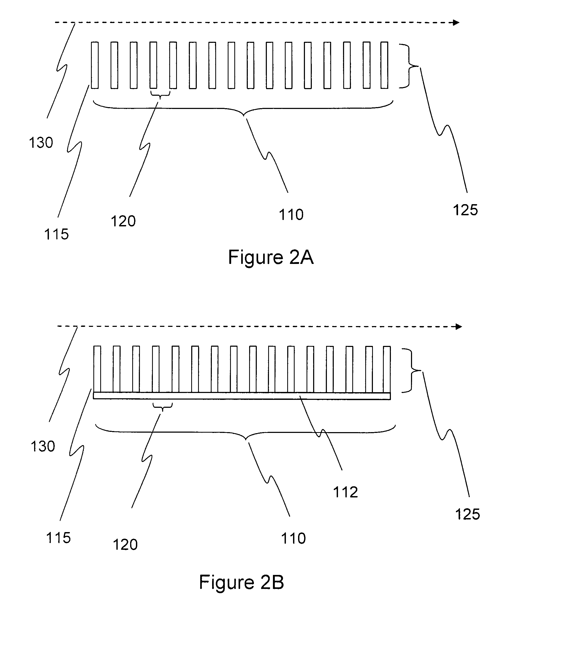
[0040] Exemplary resonant structures are illustrated in FIGS. 2A-2H. As shown in FIG. 2A, a resonant structure 110 may comprise a series of fingers 115 which ...
PUM
Abstract
Micro-resonant structures form a part of an optical interconnect system that allows various integrated circuits to communicate with each other without being connected by signal wires. Substrates have mounted thereon integrated circuits which include at least one optical communications section. Each optical communications section includes at least one transmitter and/or at least one receiver. Such transmitters may include at least one resonant structure, and such receivers may include a receiver for receiving optical emissions from at least one resonant structure. Substrates may also include, mounted thereon, at least one optical directing element such as a mirror, a lens, or a prism. Optical communications sections may also be isolated from each other using filters.
Description
CROSS-REFERENCE TO CO-PENDING APPLICATIONS [0001] The present invention is related to the following co-pending U.S. patent applications: (1) U.S. patent application Ser. No. 11 / 238,991, [atty. docket 2549-0003], entitled “Ultra-Small Resonating Charged Particle Beam Modulator,” filed Sep. 30, 2005; (2) U.S. patent application Ser. No. 10 / 917,511, filed on Aug. 13, 2004, entitled “Patterning Thin Metal Films by Dry Reactive Ion Etching;” (3) U.S. application Ser. No. 11 / 203,407, filed on Aug. 15, 2005, entitled “Method Of Patterning Ultra-Small Structures”; (4) U.S. application Ser. No. 11 / 243,476 [Atty. Docket 2549-0058], entitled “Structures And Methods For Coupling Energy From An Electromagnetic Wave,” filed on Oct. 5, 2005; (5) U.S. application Ser. No. 11 / 243,477 [Atty. Docket 2549-0059], entitled “Electron beam induced resonance,” filed on Oct. 5, 2005; (6) U.S. application Ser. No. 11 / 325,432 [Atty. Docket 2549-0021], entitled “Resonant Structure-Based Display,” filed on Jan. ...
Claims
Application Information
Patent Timeline
Application Date:The date an application was filed.
Publication Date:The date a patent or application was officially published.
First Publication Date:The earliest publication date of a patent with the same application number.
Issue Date:Publication date of the patent grant document.
PCT Entry Date:The Entry date of PCT National Phase.
Estimated Expiry Date:The statutory expiry date of a patent right according to the Patent Law, and it is the longest term of protection that the patent right can achieve without the termination of the patent right due to other reasons(Term extension factor has been taken into account ).
Invalid Date:Actual expiry date is based on effective date or publication date of legal transaction data of invalid patent.
Patent Type & Authority Applications(United States)
IPC IPC(8): H04B10/00
CPCH04B10/803H01J25/00
Inventor GORRELL, JONATHANDAVIDSON, MARKMAINES, MICHAEL E.