High density integrated circuit apparatus, test probe and methods of use thereof

a technology of integrated circuits and test probes, which is applied in the direction of soldering apparatus, instruments, and semiconductor/solid-state device details, etc., can solve the problems of high cost of fabrication of integrated circuit probes, easy damage of wires, so as to achieve high-performance functional testing and high temperature burn

Inactive Publication Date: 2007-11-29
GLOBALFOUNDRIES INC
View PDF99 Cites 109 Cited by
  • Summary
  • Abstract
  • Description
  • Claims
  • Application Information

AI Technical Summary

Benefits of technology

[0009] It is an additional object of the present invention to provide probes having contacts which c

Problems solved by technology

Testing is an expensive part of the fabrication process of contemporary computing systems.
The functionality of every I/O for contemporary integrated circuit must be tested since a failure to achieve the design specification at a single I/O can render an integrated circuit unusable for a specific application.
Contemporary probes for integrated circuits are expensive to fabricate and are easily damaged.
The wires are generally fragile and easily damage and are easily displaceable from the predetermined positions corresponding to the design positions of the contact locations o

Method used


Image

  • High density integrated circuit apparatus, test probe and methods of use thereof
  • High density integrated circuit apparatus, test probe and methods of use thereof
  • High density integrated circuit apparatus, test probe and methods of use thereof

Examples


Embodiment Construction

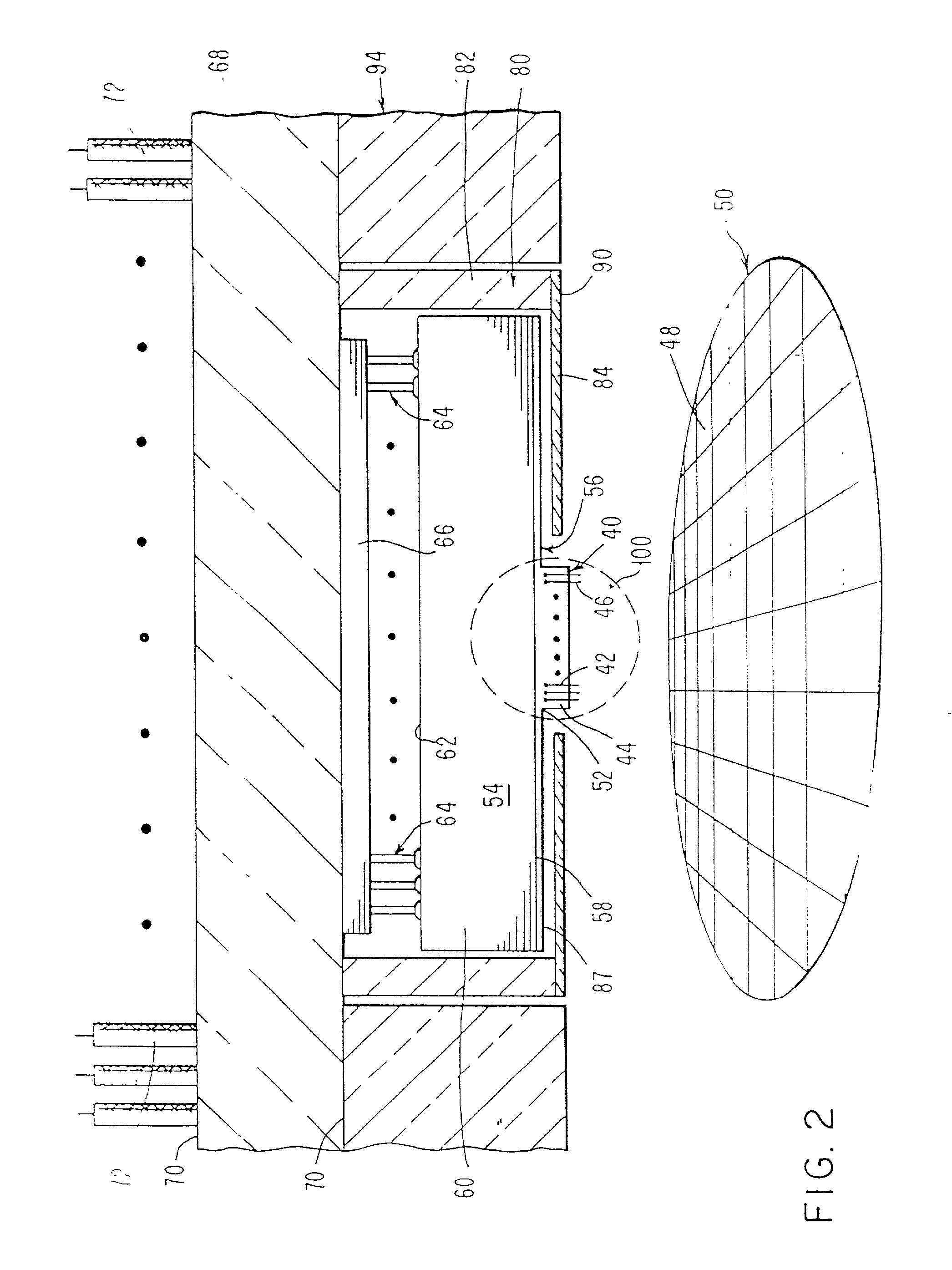
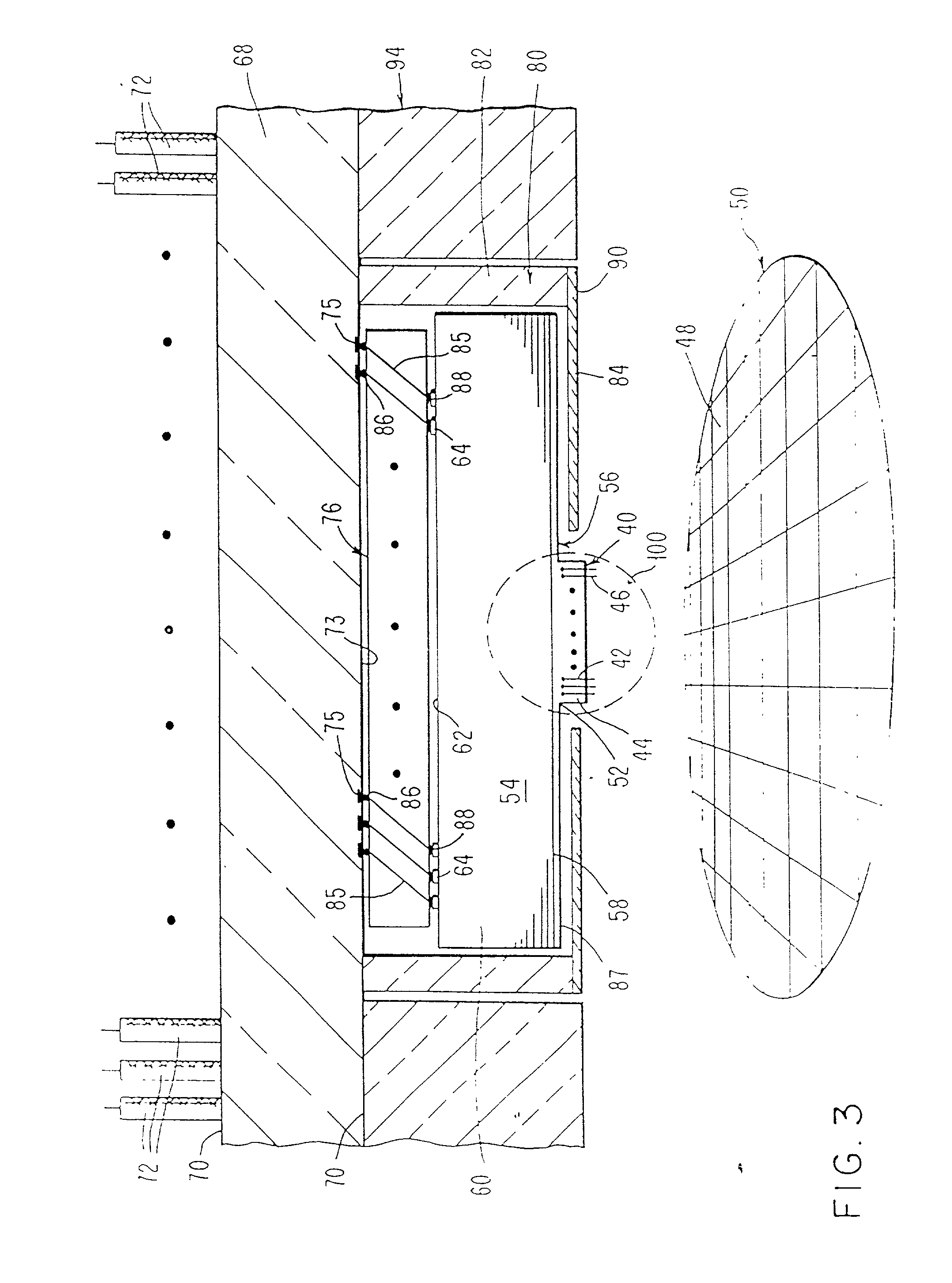
[0033] Turning now to the figures, FIGS. 2 and 3 show two embodiments of the test assembly according to the present invention. Numerals common between FIGS. 2 and 3 represent the same thing. Probe head 40 is formed from a plurality of elongated electrically conducting members 42 embedded in a material 44 which is preferably an elastomeric material 44. The elongated conducting members 42 have ends 46 for probing contact locations on integrated circuit devices 48 of wafer 50. In the preferred embodiment, the workpiece is an integrated circuit such as a semiconductor chip or a semiconductor wafer having a plurality of chips. The workpiece can be any other electronic device. The opposite ends 52 of elongated electrical conductors 42 are in electrical contact with space transformer (or fan-out substrate) 54. In the preferred embodiment, space transformer 54 is a multilevel metal / ceramic substrate, a multilevel metal / polymer substrate or a printed circuit board which are typically used as...


PUM

PropertyMeasurementUnit
Temperatureaaaaaaaaaa
Elastomericaaaaaaaaaa
Densityaaaaaaaaaa

Abstract

The present invention is directed to a high density test probe which provides a means for testing a high density and high performance integrated circuits in wafer form or as discrete chips. The test probe is formed from a dense array of elongated electrical conductors which are embedded in an compliant or high modulus elastomeric material. A standard packaging substrate, such as a ceramic integrated circuit chip packaging substrate is used to provide a space transformer. Wires are bonded to an array of contact pads on the surface of the space transformer. The space transformer formed from a multilayer integrated circuit chip packaging substrate. The wires are as dense as the contact location array. A mold is disposed surrounding the array of outwardly projecting wires. A liquid elastomer is disposed ion the mold to fill the spaces between the wires. The elastomer is cured and the mold is removed, leaving an array of wires disposed in the elastomer and in electrical contact with the space transformer The space transformer can have an array of pins which are on the opposite surface of the space transformer opposite to that on which the elongated conductors are bonded. The pins are inserted into a socket on a second space transformer, such as a printed circuit board to form a probe assembly. Alternatively, an interposer electrical connector can be disposed between the first and second space transformer.

Description

FIELD OF THE INVENTION [0001] This invention relates to an apparatus and test probe for integrated circuit devices and methods of use thereof. BACKGROUND OF THE INVENTION [0002] In the microelectronics industry, before integrated circuit (IC) chips are packaged in an electronic component, such as a computer, they are tested. Testing is essential to determine whether the integrated circuit's electrical characteristics conform to the specifications to which they were designed to ensure that electronic component performs the function for which it was designed. [0003] Testing is an expensive part of the fabrication process of contemporary computing systems. The functionality of every I / O for contemporary integrated circuit must be tested since a failure to achieve the design specification at a single I / O can render an integrated circuit unusable for a specific application. The testing is commonly done both at room temperature and at elevated temperatures to test functionality and at ele...

Claims


Application Information

Patent Timeline
IPC IPC(8): H05K3/00G01R1/00H01R9/00H01L23/52G01R1/067G01R1/073G01R3/00G01R31/28H01L23/498H01L23/538H01L25/065H01L25/07H01L25/18
CPCG01R1/06711Y10T29/49147G01R1/07307G01R1/07314G01R1/07342G01R1/07371G01R1/07378G01R3/00G01R31/2886H01L23/49827H01L23/5384H01L25/0652H01L2224/1134H01L2224/16H01L2224/78301H01L2924/01014H01L2924/01046H01L2924/01078H01L2924/01079H01L2924/09701H01L2924/3011H01L2224/13099H01L2924/00013H01L2924/01019G01R1/0675Y10T29/49162Y10T29/53174Y10T29/49192H01L2924/10253Y10S29/029Y10T29/49004Y10T29/49158Y10T29/49126Y10T29/49149H01L2924/00H01L24/45H01L24/48H01L2224/45015H01L2224/45124H01L2224/45144H01L2224/45147H01L2224/45155H01L2224/45164H01L2224/48091H01L2224/48227H01L2224/85205H01L2224/85214H01L2924/15192H01L2924/19107H01L2924/12042H01L2924/14H01L2924/1627H01L2924/181H01L2924/00014H01L2924/20752H01L2924/20753H01L2924/20754H01L2924/20755H01L2924/20756H01L2924/20757H01L2924/20758H01L2924/20759H01L2924/2076
Inventor BEAMAN, BRIAN SAMUELFOGEL, KEITH EDWARDLAURO, PAUL ALFREDNORCOTT, MAURICE HEATHCOTESHIH, DA-YUANWALKER, GEORGE FREDERICK
Owner GLOBALFOUNDRIES INC
Why Eureka
Try Eureka