Electrostatic Chuck And Chuck Base Having Cooling Path For Cooling Wafer

Inactive Publication Date: 2007-11-29
ADAPTIVE PLASMA TECH
View PDF4 Cites 10 Cited by
  • Summary
  • Abstract
  • Description
  • Claims
  • Application Information

AI Technical Summary

Benefits of technology

[0009] Therefore, the present invention has been made in view of the above problems, and it is an object of the present invention to provide an electrostatic chuck having a cooling channel that is cap

Problems solved by technology

When the temperature of the entire wafer is not uniformly maintained, defectiveness, such as poor distribution of critical dimensions on the wafer is generated during the etching process.
However, application of such high direct current voltage l

Method used


Image

  • Electrostatic Chuck And Chuck Base Having Cooling Path For Cooling Wafer
  • Electrostatic Chuck And Chuck Base Having Cooling Path For Cooling Wafer
  • Electrostatic Chuck And Chuck Base Having Cooling Path For Cooling Wafer

Examples


Embodiment Construction

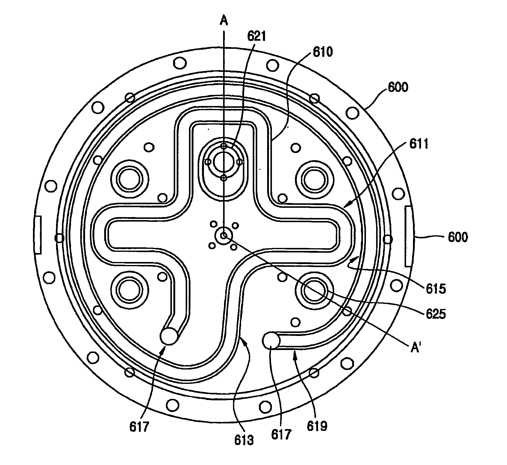
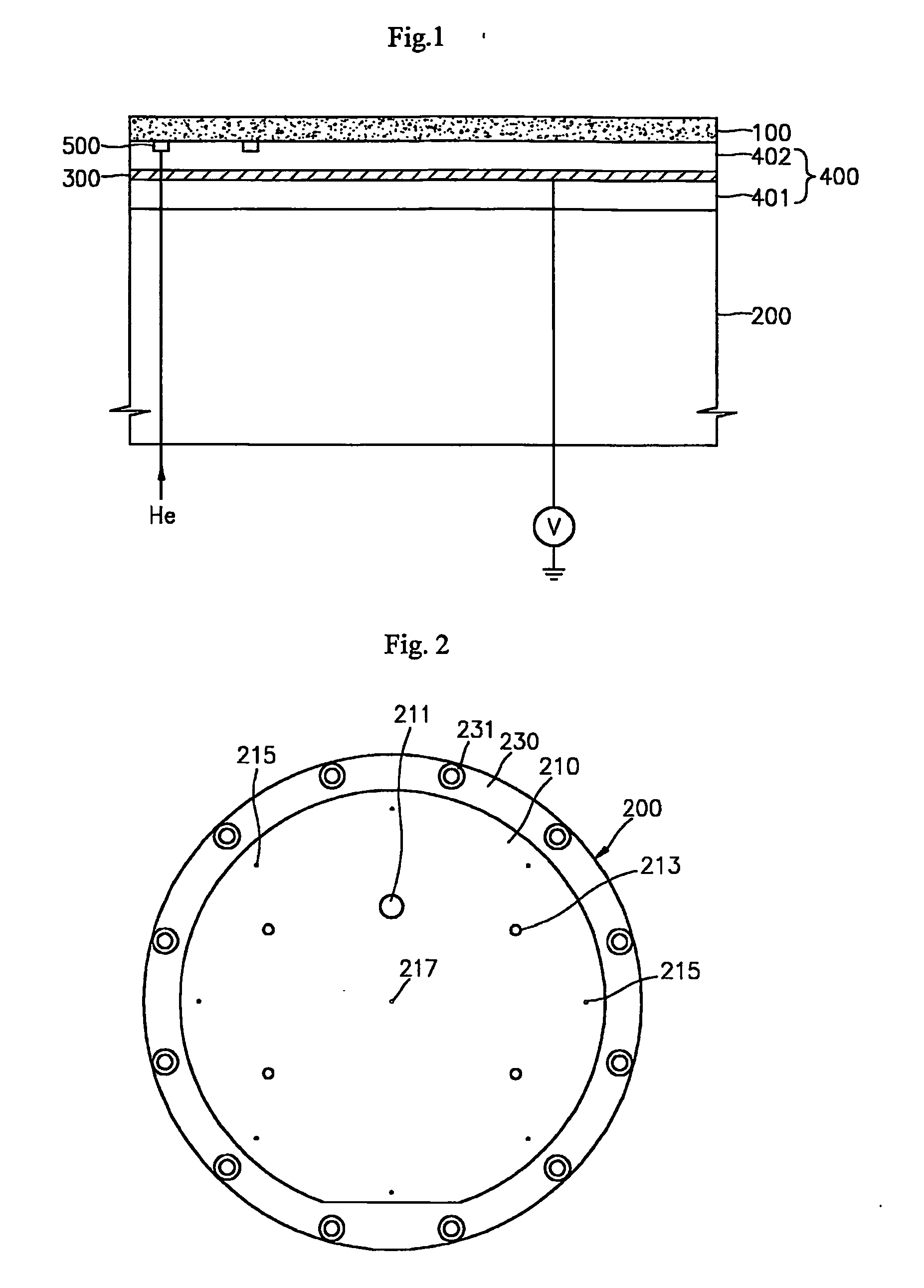
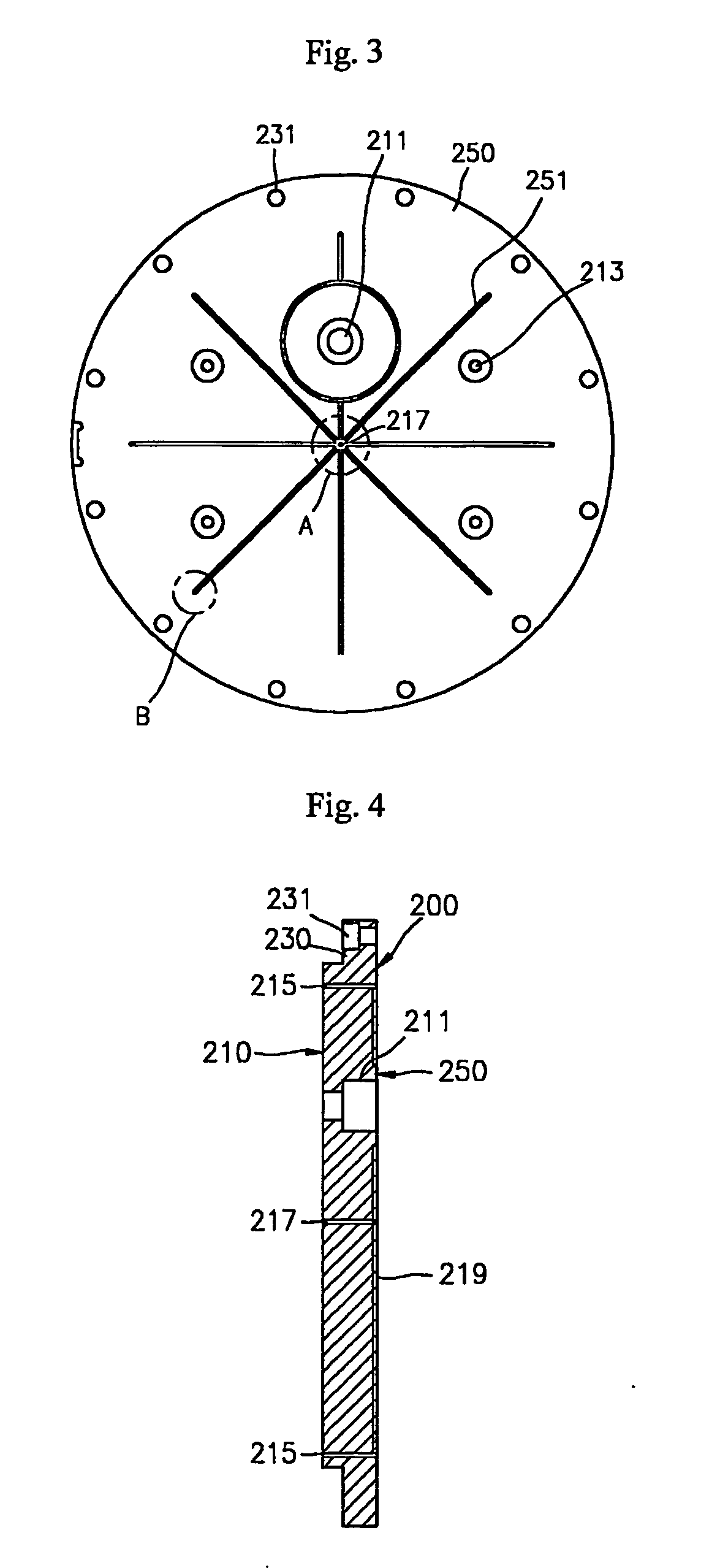
[0036] An electrostatic chuck according to a preferred embodiment of the present invention is schematically shown in FIGS. 1 to 14.

[0037]FIG. 1 shows the structure of the electrostatic chuck according to the preferred embodiment of the present invention.

[0038] Referring to FIG. 1, the electrostatic chuck according to the preferred embodiment of the present invention comprises a chuck base 200 for supporting a wafer 100, on which an etching process is performed. Under the chuck base 200 may be disposed a chuck body (not shown) for supporting the chuck base 200.

[0039] On the chuck base 200 is formed a dielectric film 400. Generally, the dielectric film 400 may be formed by anodizing. In the preferred embodiment of the present invention, however, an additional dielectric sheet, which is manufactured in the shape of a sheet, is attached to the surface of the chuck base 200 while being compressed. In the illustrated embodiment, the dielectric sheet comprises a first dielectric sheet p...


PUM


Abstract

The electrostatic chuck comprises a chuck base for supporting a wafer, a dielectric film mounted on the chuck base, the dielectric film having an electrode for supplying direct current voltage to provide an electrostatic force to fix the wafer, the electrode disposed in the dielectric film, and a cooling channel for supplying refrigerant to the dielectric film to control the temperature of the wafer. At least two first cooling channel parts are formed at the surface of the dielectric film corresponding to the edge part of the wafer such that the first cooling channel parts form concentric circles, second cooling channel parts formed at the surface of the dielectric film such that the first cooling channel parts are connected to each other through the second cooling channel parts, first through channels formed through the dielectric film for supplying the refrigerant to the first and second cooling channel parts, and a second through channel formed through the center of the dielectric film for supplying the refrigerant to the center of the wafer.

Description

TECHNICAL FIELD [0001] The present invention relates to semiconductor device manufacturing equipment, and, more particularly, to an electrostatic chuck (ESC) and a chuck base having a cooling path or channel for cooling a wafer. BACKGROUND ART [0002] In a reaction chamber of semiconductor device manufacturing equipment, for example, a dry etcher, is mounted a chuck for supporting a semiconductor wafer during a process. The chuck may be an electrostatic chuck. The chuck is mounted on a chuck base, which is disposed at the rear surface of the chuck. The chuck base serves to support the chuck. The chuck base is provided with a cooling channel for maintaining a constant temperature of the chuck, and therefore, uniformly cooling the semiconductor wafer located on the chuck. [0003] The electrostatic chuck fixes the wafer using an electrostatic force. To this end, the electrostatic chuck has a structure for generating an electrostatic force or electrostatic adsorptive force, for example, a...

Claims


Application Information

Patent Timeline
IPC IPC(8): H01L21/3065H01L21/00H01L21/683
CPCH01L21/6831H01L21/67109H01L21/3065
Inventor PARK, HEE YONGKIM, JIN TAILEE, KYU HAPARK, KWAN TAEOH, SANG YOUNGJANG, HWI GON
Owner ADAPTIVE PLASMA TECH
Why Eureka
Try Eureka