Electronic Component Mounting Structure

Inactive Publication Date: 2007-11-29
HENKEL JAPAN
View PDF3 Cites 4 Cited by
  • Summary
  • Abstract
  • Description
  • Claims
  • Application Information

AI Technical Summary

Benefits of technology

[0018]The present invention is capable of providing an electronic component mounting structure having no degradation of bonding reliability and small warpage at the same time even when a die becomes larger in a mounting structure including a semiconductor device carrying a flip-chip mounting.

Problems solved by technology

As the size of a semiconductor die becomes larger, however the problem of warpage of a mounting structure packed on a substrate arises in addition to the problem of segregation and resultant disconnection, and these problems need to be resolved with consideration of their balance.

Method used


Image

  • Electronic Component Mounting Structure
  • Electronic Component Mounting Structure
  • Electronic Component Mounting Structure

Examples


example 1

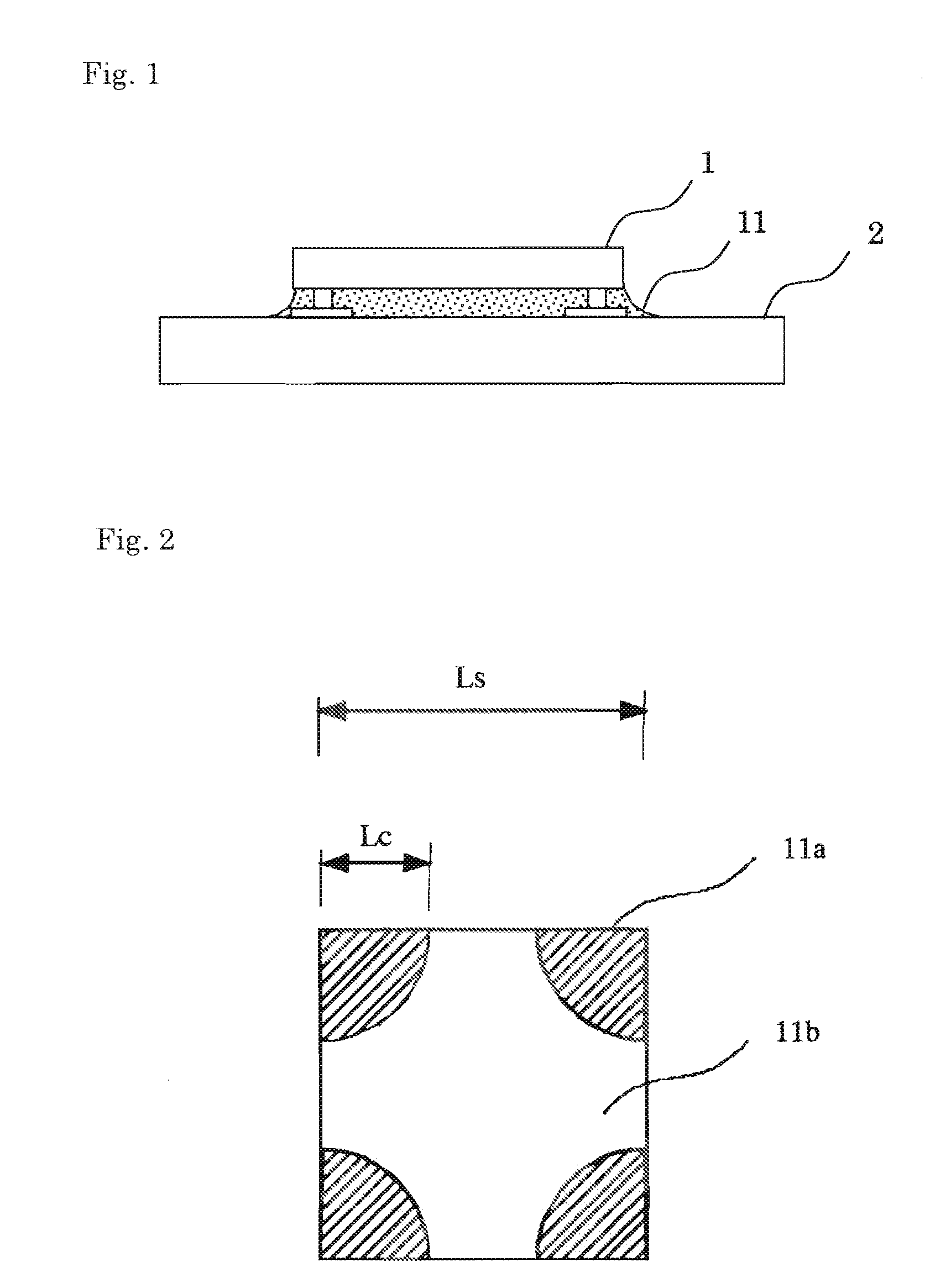
[0054]At the center of the place on where an electronic component is supposed to be mounted, about 6 mg of the above-mentioned resin composition B was applied on a printed circuit board in which electrode surfaces were plated with Au / Ni (glass epoxy board FR-4 0.1 mm thick, copper foil 18 μm thick). Then, about 4 mg in the total of the above-mentioned resin composition A was applied at the positions corresponding to the four corners of an electronic component. Subsequently, onto that place the silicon chip equipped with copper-plated bumps around its periphery and having 10 mm×10 mm×0.3 mm in size (size of gold stud bump: 50 μm×50 μm×25 μm, number of bump: 200, pitch of bump: 120 μm to 200 μm), as an electronic component, was bonded by application of heat and pressure by using a bonding machine for 4 seconds under the condition of 240° C. and 15 kg / cm2. Thus, a sample piece for determining properties was obtained.

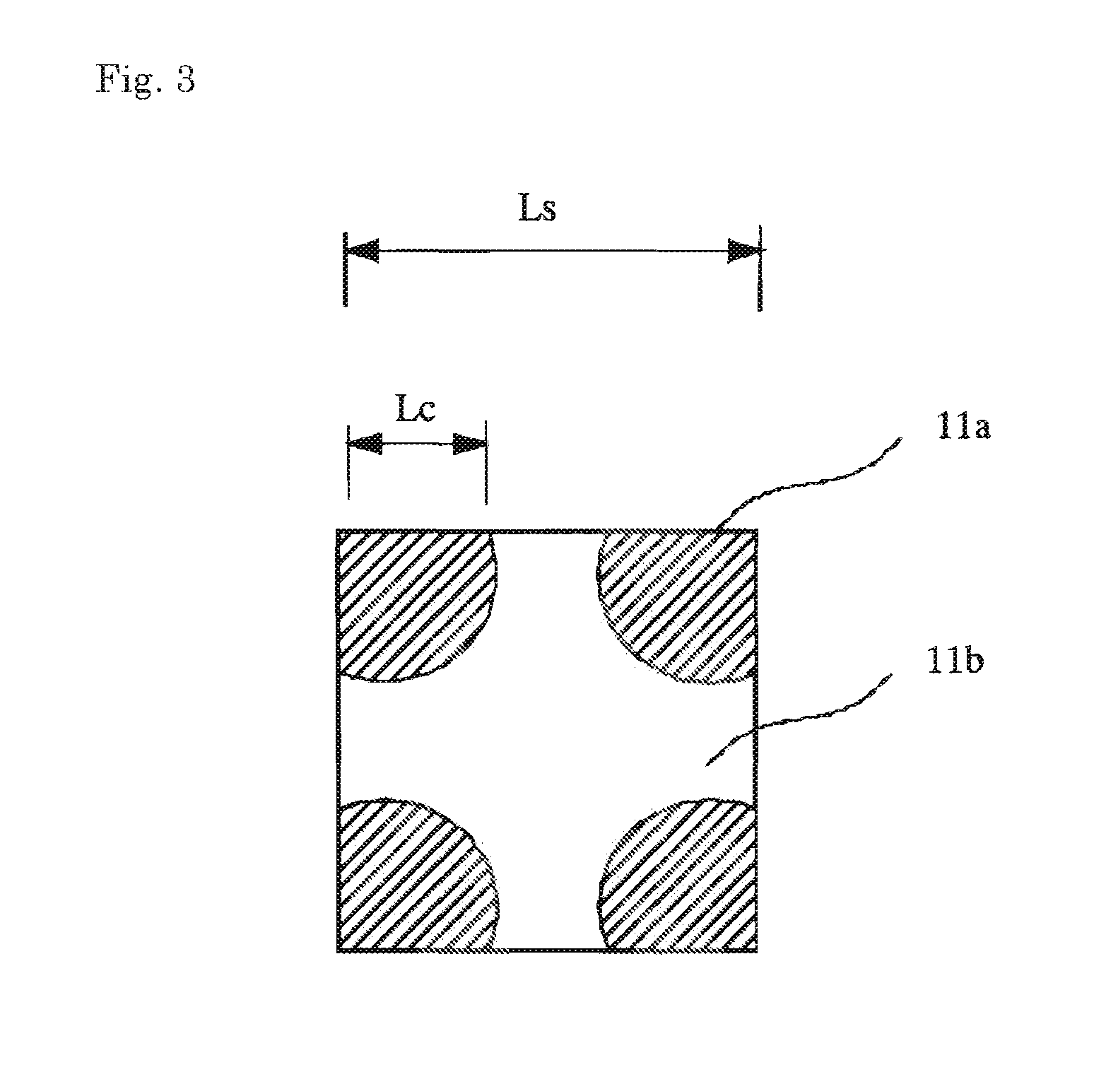
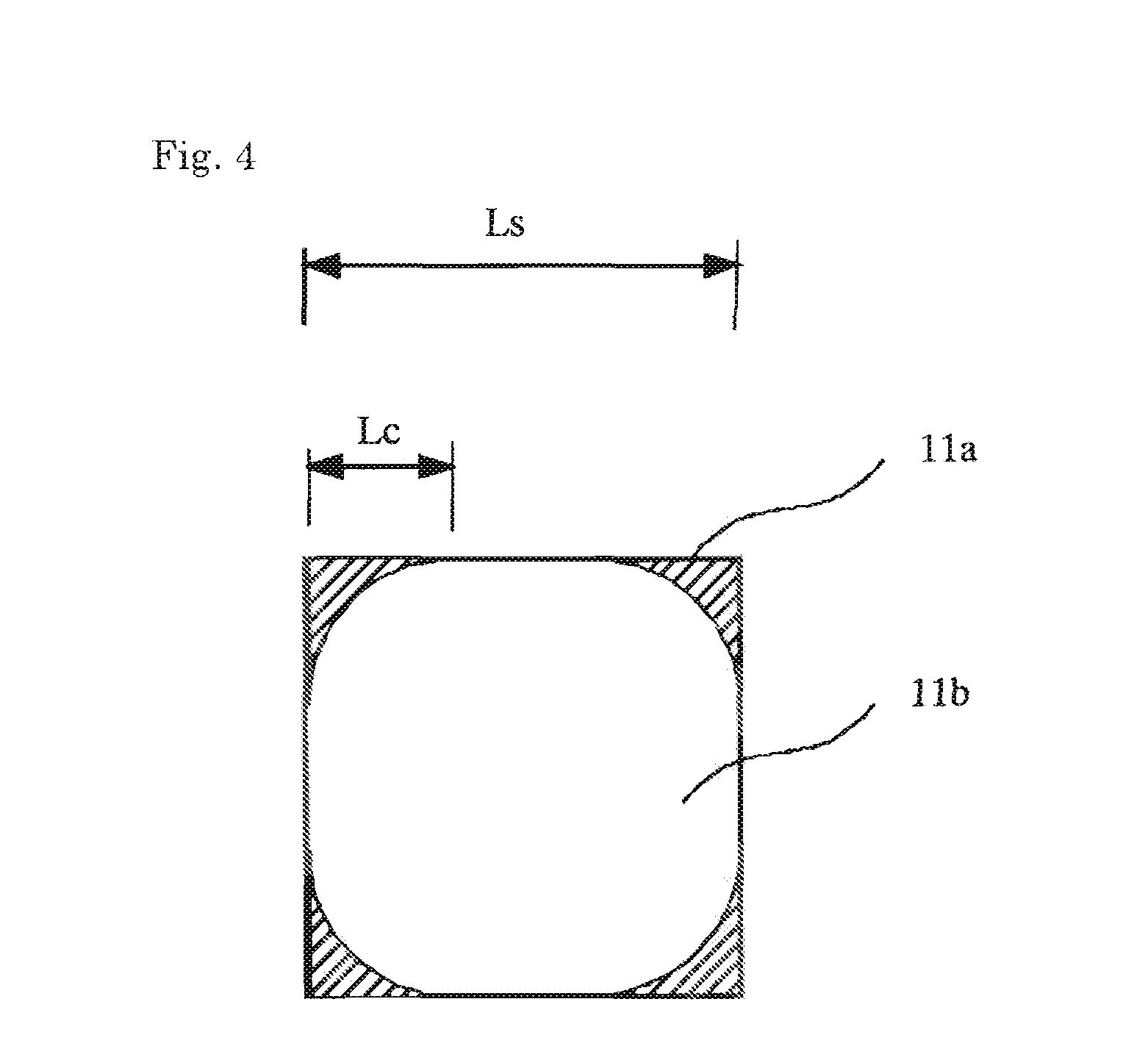
[0055]The shape of the first cured resin filling under the electronic ...


PUM

PropertyMeasurementUnit
flexural modulusaaaaaaaaaa
temperatureaaaaaaaaaa

Abstract

An object of the present invention is to provide an electronic component mounting structure having no degradation of bonding reliability and small warpage at the same time even when a die becomes more extensive in a mounting structure including a semiconductor device carrying a flip-chip mounting.
Such electronic component mounting structure comprises a substrate and a quadrate electronic component mounted on the substrate, wherein a gap between the substrate and the electronic component is filled with a first cured resin filling at least a corner area of the electronic component and a second cured resin filling at least a center area of the electronic component, and a flexural modulus of the first cured resin is higher than a flexural modulus of the second cured resin.

Description

TECHNICAL FIELD[0001]The present invention relates to an electronic component mounting structure used in an electronic device, and particularly to a semiconductor mounting structure in which a semiconductor die is mounted on a substrate.BACKGROUND ART[0002]While semiconductor elements become larger as recent progress in the technology in the field of manufacturing electronic devices, flip-chip mountings, in which semiconductor elements are face-down packed and bonded onto a wiring substrate, have been increasingly employed in order to meet the requirement of reducing electronic devices in size and weight.[0003]In flip-chip mountings, a convex called “bump” is typically set up at an electrode of semiconductor elements, and each electrode is bonded in ways that the bump is face-down opposed to a wiring substrate, which characteristically enables high density mounting compared to wire-bonding mountings. Various designs of flip-chip mountings are known; for example, a bump set up on a w...

Claims


Application Information

Patent Timeline
Patent Type & Authority Applications(United States)
IPC IPC(8): H01L21/56B32B27/00
CPCH01L21/563H01L24/81H01L2924/10253H01L2224/32225H01L24/29H01L2924/01087H01L2924/01045H01L2924/01033H01L2924/01006H01L2924/01079H01L2924/01078H01L2924/0105H01L2224/16225H01L2224/73203H01L2224/73204H01L2224/81203H01L2224/81801H01L2224/83102H01L2224/83194H01L2224/92125H01L2924/01004H01L2924/01005H01L2924/01012H01L2924/01027H01L2924/01029H01L2924/00H01L2924/351H01L2924/15787
Inventor KISHIMOTO, YASUKAZU
Owner HENKEL JAPAN
Why Eureka
Try Eureka