Semiconductor device

a technology of semiconductors and devices, applied in the direction of transistors, diodes, electrical devices, etc., can solve the problems of reducing the temperature of the device, and achieve the effect of high voltage and high thermal conductivity

Active Publication Date: 2007-12-06
CREE SWEDEN
View PDF10 Cites 25 Cited by
  • Summary
  • Abstract
  • Description
  • Claims
  • Application Information

AI Technical Summary

Benefits of technology

[0020]Such devices of SiC or diamond are particularly interesting for high power applications, especially when they have to be switched on and off at high frequencies due to the possibility of making th

Problems solved by technology

This results in the problems discussed above to obtain a sufficient voltage between said additional layers 7′ and drift layer portions close thereto upon surge for cr

Method used


Image

  • Semiconductor device
  • Semiconductor device

Examples


first embodiment

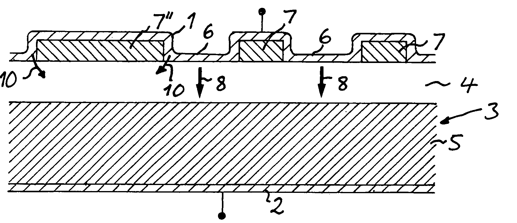
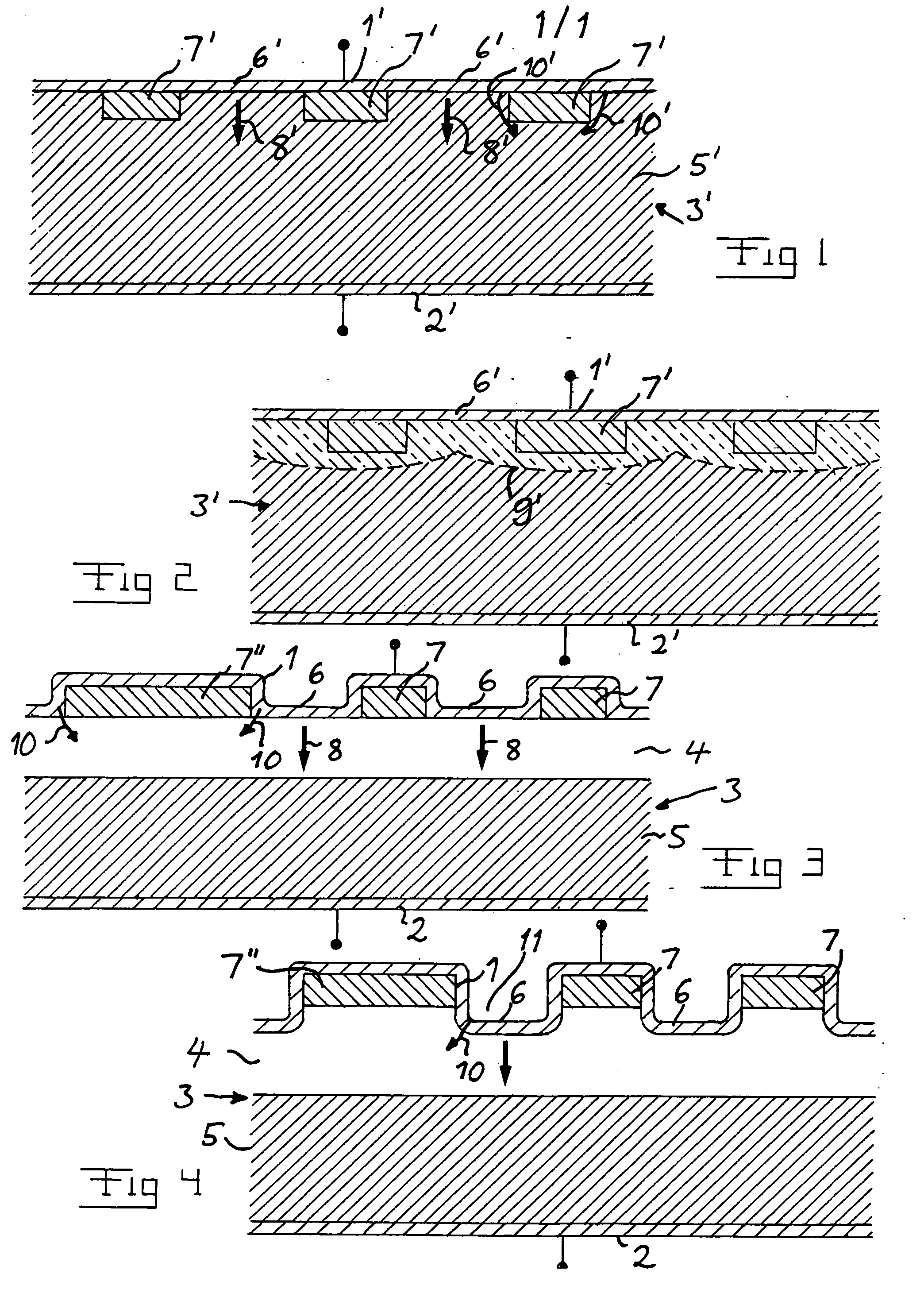
[0031]The present invention addresses this problem, and a device according to the invention is schematically shown in FIG. 3. Parts of this device corresponding to parts of the prior art device according to FIGS. 1 and 2 have been provided with the same reference numerals. The semiconductor material of this device is SiC. This device differs from known such devices by the fact that the drift layer 3 has two sub-layers, namely a first low doped sub-layer 4 closest to the source contact and a lower highly doped second sub-layer 5 closest to the drain contact and that at least one said additional layer 7″ has a substantially larger lateral extension and thereby larger area of the interface to the drift layer than adjacent such layers 7. Said additional layers and the Schottky-contact regions 6 are in the present case arranged on top of the drift layer 3 in the form of concentric rings each having a substantially constant width and said lateral extension means the direction according to...

second embodiment

[0034]FIG. 4 illustrates a device according to the invention differing from the one shown in FIG. 3 by the arrangement of the Schottky-contact regions 6 at the bottom of a recess or trench 11 into the drift layer each separating adjacent said additional layers and positioning said Schottky-contacts at a vertical distance to the interfaces between said additional layers 7, 7″ and the drift layer. This vertical distance between the Schottky-contacts and said interface means that electrons injected into the drift layer from the Schottky-contacts upon surge will disturb the building-up of a sufficient voltage between the additional layers 7, 7″ and the drift layer for hole injection into the drift layer. The width of said at least one additional layer is in this embodiment two times the width of adjacent additional layers 7, which means that said voltage will upon surge be easier and faster built-up for the additional layer 7″ than for the other additional layers 7.

[0035]A difference be...


PUM


Abstract

A semiconductor device of unipolar type has Schottky-contacts (6) laterally separated by regions in the form of additional layers (7, 7″) of semiconductor material on top of a drift layer (3). Said additional layers being doped according to a conductivity type being opposite to the one of the drift layer. At least one (7″) of the additional layers has a substantially larger lateral extension and thereby larger area of the interface to the drift layer than adjacent such layers (7) for facilitating the building-up of a sufficient voltage between that layer and the drift layer for injecting minority charge carriers into the drift layer upon surge for surge protection.

Description

TECHNICAL FIELD OF THE INVENTION AND PRIOR ART[0001]The present invention relates to a semiconductor device having a source contact and a drain contact interconnected by a drift layer doped by dopants according to a first conductivity type, n or p, for majority charge carrier transport in a conducting path between the source contact and the drain contact in a forward biased state of the device, said device comprising on top of the drift layer a plurality of metal layer regions belonging to the source contact making Schottky-contacts to the drift layer and being laterally separated by regions in the form of additional layers of semiconductor material on top of said drift layer and doped by dopants according to a second conductivity type being opposite to said first type for forming pn-junctions at the interface thereof to the drift layer and adapted to form a continuous blocking pn-junction in the reverse biased state of the device shielding said Schottky-contact regions, said source...

Claims


Application Information

Patent Timeline
IPC IPC(8): H01L29/47H01L27/095
CPCH01L21/8213H01L27/0255H01L27/0814H01L29/872H01L29/1602H01L29/1608H01L29/8611H01L29/16H01L29/0619
Inventor HARRIS, CHRISTOPHERBASCERI, CEMBERTILSSON, KENT
Owner CREE SWEDEN
Why Eureka
Try Eureka