Dual surface SOI by lateral epitaxial overgrowth

a technology of lateral epitaxial overgrowth and soi, applied in the field of high-performance field-effect transistors, can solve the problems of layout and design penalties, the redesign and integration development cost of overcoming the performance limitations of bulk silicon can be substantial, and the performance of soi substrates can be degraded

Inactive Publication Date: 2007-12-06
NORTH STAR INNOVATIONS
View PDF7 Cites 94 Cited by
  • Summary
  • Abstract
  • Description
  • Claims
  • Application Information

AI Technical Summary

Problems solved by technology

Prior attempts to integrate dual or hybrid substrates have used bulk silicon to form at least one of the PMOS and NMOS substrates, resulting in degraded performance compared to SOI substrates.
The redesign and integration development costs of overcoming the performance limitations of bulk silicon can be substantial.
In addition, when bulk silicon (or, for that matter, SOI silicon) is used as a single orientation surface to form FinFET CMOS devices, a forty-five degree alignment is required between NMOS and PMOS devices, creating layout and design penalties.
While fully SOI dual surface orientation (DSO) integrations have been proposed to address some of these drawbacks, such integrations are overly complex, use inferior semiconductor substrate formation processes (e.g., using SIMOX techniques), use complicated substrate structures (e.g., wafer bonding), and / or do not maintain planarity between regions of different crystallographic orientation.

Method used


Image

  • Dual surface SOI by lateral epitaxial overgrowth
  • Dual surface SOI by lateral epitaxial overgrowth
  • Dual surface SOI by lateral epitaxial overgrowth

Examples


Embodiment Construction

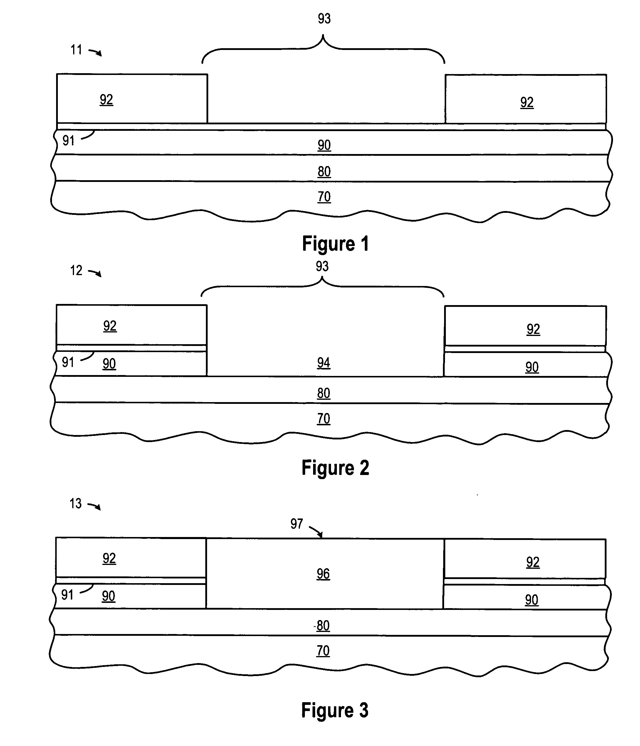
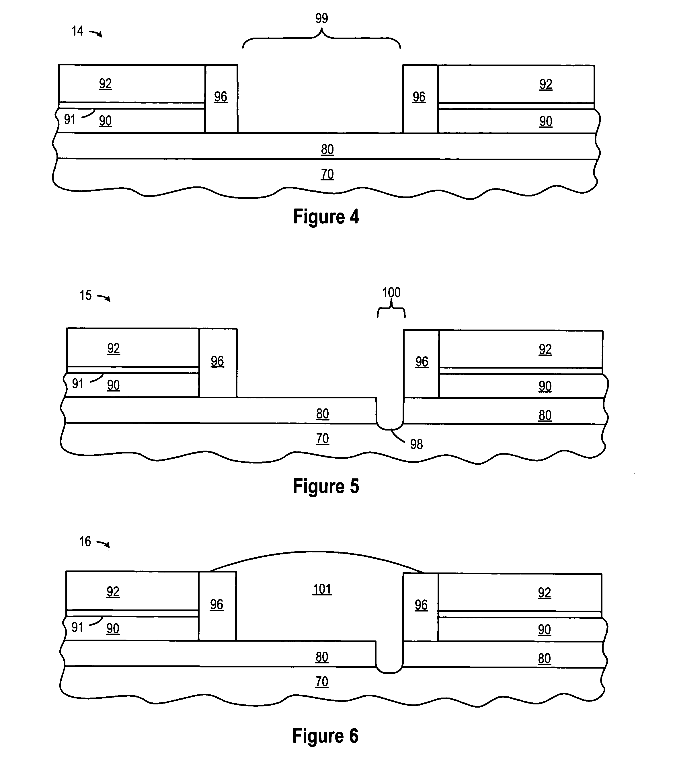
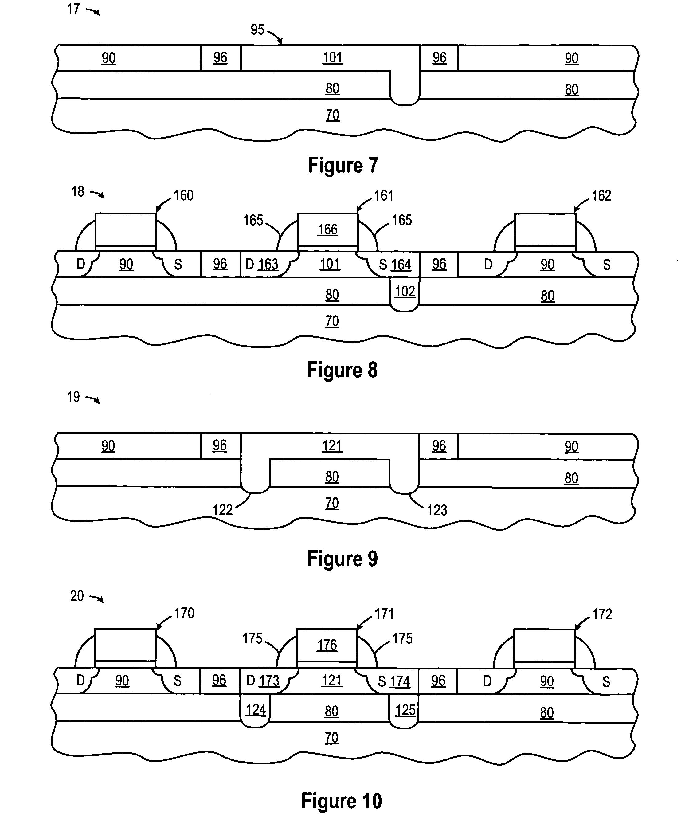
[0030]A method and apparatus are described for fabricating high performance CMOS devices with hybrid or dual surface orientations using lateral epitaxial overgrowth to form SOI and quasi SOI CMOS devices. Using lateral epitaxial overgrowth from one or more seed areas in an underlying bulk semiconductor substrate, semiconductor layers or seed regions can be grown from the bulk semiconductor and over an insulator layer to form SOI substrates. Depending on the size and configuration of the seed regions, the SOI devices (e.g., MOSFET transistors) formed over the overgrown semiconductor layers may be placed so that at least the source region (if not also the channel region) is located over the seed region, though the drain region may also be located over a seed region when multiple seed regions are formed. In addition or in the alternative, SOI devices formed over the overgrown semiconductor layers may be placed so that the drain region is located over a buried oxide layer, thereby reduc...


PUM


Abstract

A semiconductor process and apparatus provide a planarized hybrid substrate (18) by exposing a buried oxide layer (80) in a first area (99), selectively etching the buried oxide layer (80) to expose a first semiconductor layer (70) in a second smaller seed area (98), and then epitaxially growing a first epitaxial semiconductor material from the seed area (98) of the first semiconductor layer (70) that fills the second trench opening (100) and grows laterally over the exposed insulator layer (80) to fill at least part of the first trench opening (99), thereby forming a first epitaxial semiconductor layer (101) that is electrically isolated from the second semiconductor layer (90). By forming a first SOI transistor device (160) over a first SOI layer (90) using deposited (100) silicon and forming first SOI transistor (161) over an epitaxially grown (110) silicon layer (101), a high performance CMOS device is obtained.

Description

BACKGROUND OF THE INVENTION[0001]1. Field of the Invention[0002]The present invention is directed in general to the field of semiconductor devices. In one aspect, the present invention relates to high-performance field effect transistors (FETs) fabricated on hybrid or dual substrates.[0003]2. Description of the Related Art[0004]To address the difference in electron and hole mobility values for NMOS and PMOS transistor devices formed on semiconductor wafers having a single crystal orientation, integrated circuit devices are increasingly fabricated with hybrid substrates with different surface orientations using semiconductor-on-insulator (SOI) wafer bonding to provide PMOS and NMOS devices with their own optimized crystal orientation. Prior attempts to integrate dual or hybrid substrates have used bulk silicon to form at least one of the PMOS and NMOS substrates, resulting in degraded performance compared to SOI substrates. For example, bulk silicon substrates have increased junction...

Claims


Application Information

Patent Timeline
Patent Type & Authority Applications(United States)
IPC IPC(8): H01L21/20
CPCH01L21/84H01L27/1203H01L27/1207H01L29/785H01L29/045
Inventor WINSTEAD, BRIAN A.ZIA, OMARSADAKA, MARIAM G.ORLOWSKI, MARIUS K.
Owner NORTH STAR INNOVATIONS
Why Eureka
Try Eureka