Multilayer Substrate Manufacturing Method

Inactive Publication Date: 2007-12-06
SANYO ELECTRIC CO LTD
View PDF4 Cites 11 Cited by
  • Summary
  • Abstract
  • Description
  • Claims
  • Application Information

AI Technical Summary

Benefits of technology

[0019] According to the manufacturing method of a multilayer substrate of some embodiments of the invention, the position of the positioning section provided in a conductive film formed at the beginning is identified to carry out patterning of a second and/or any subsequent films. Thus, even in case a plurality of wiring layers are formed, position identification is carried out by one of the positioning sections formed at the beginning so that accuracy of the relative positioning of layers can be improved. Moreover, patterning of the interconnecting portion connecting wiring layers is carried out after identifying the position of the positioning section. It is thus possible to improve positioning accuracy at locations where interconnecting po

Problems solved by technology

In the above-described method, deviations in the positioning of the wiring layers occur and it is diff

Method used


Image

  • Multilayer Substrate Manufacturing Method
  • Multilayer Substrate Manufacturing Method
  • Multilayer Substrate Manufacturing Method

Examples


Embodiment Construction

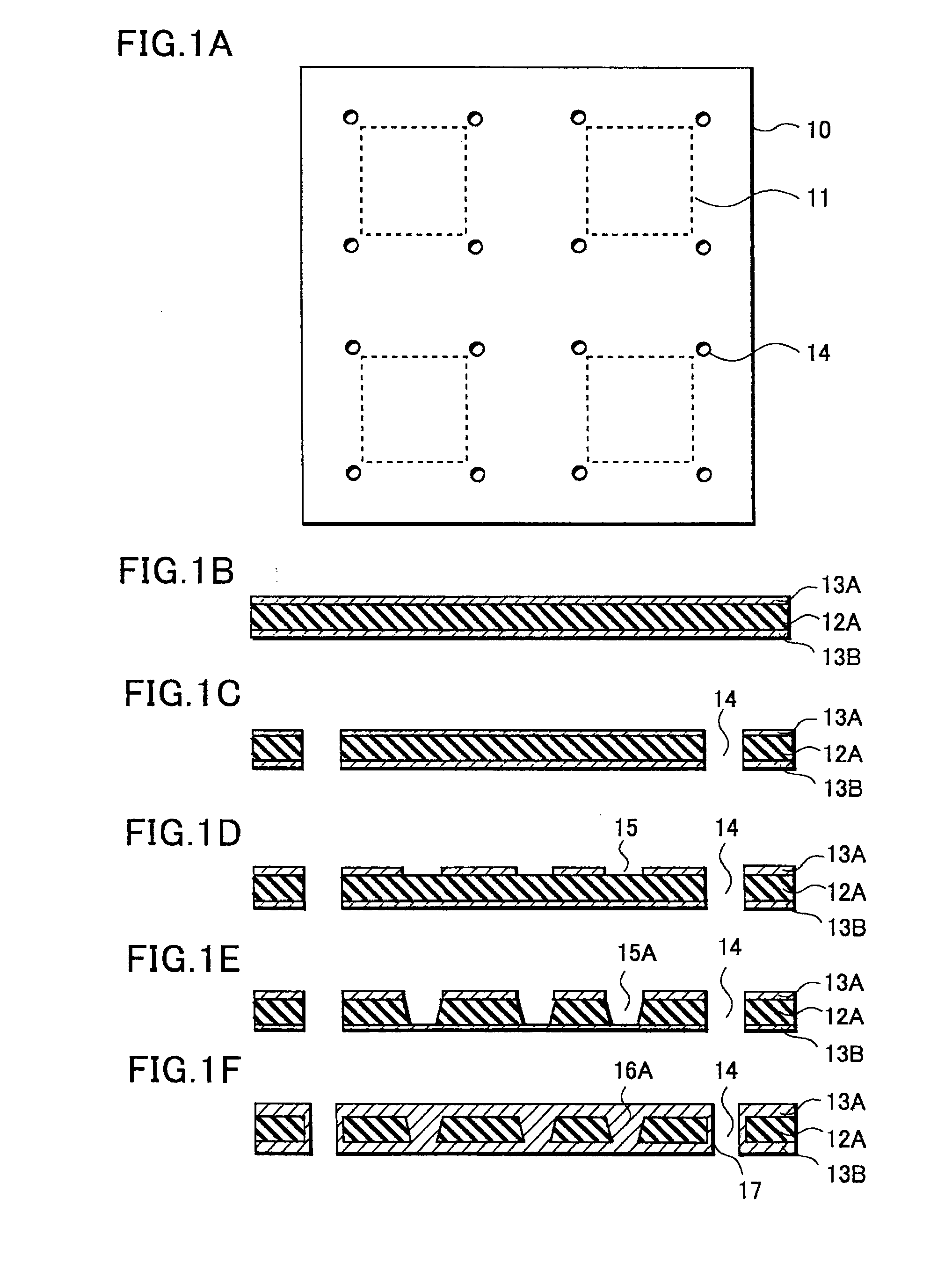
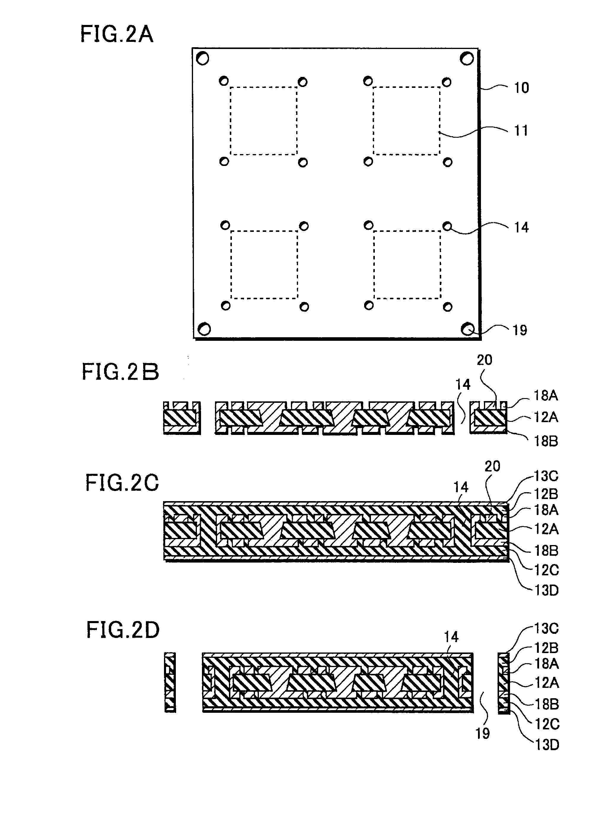
[0030] A manufacturing method of a multilayer substrate according to some preferred embodiments is described with reference to several figures. In the present embodiment, multilayer wiring indicate a wiring structure having two or more layers and corresponds to a substrate comprising multilayer wiring or a multilayer substrate, etc. mounting a circuit device for a package.

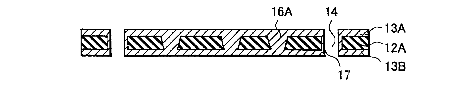
[0031] In the manufacturing method of this preferred embodiment, the multilayer substrate to be manufactured comprises a wiring layer 18 formed by patterning a conductive film 13 and laminated via an insulating film 12 and after providing positioning holes 14 in the conductive film 13 laminated at the beginning and identifying the positioning thereof, the second and / or any subsequent wiring layers 18 is / are patterned. Here, an interconnection portion 16 connecting wiring layers can be formed using the positioning hole (positioning section).

[0032]FIG. 1 shows the process of forming positioning holes 14 in a lamina...


PUM

PropertyMeasurementUnit
Electrical conductoraaaaaaaaaa

Abstract

A manufacturing method of a multilayer substrate that suppresses relative displacement of layers and forms interconnecting portions electrically connecting layers having an accurate positioning. A manufacturing method of a multilayer substrate for laminating, via an insulating film, a wiring layer formed by patterning a conductive film comprises providing a positioning hole in a conductive film laminated at the beginning and patterning a second and/or any subsequent wiring layers after identifying a position of an identification section. Interconnecting sections for interconnecting wiring layers are formed using the identification section.

Description

[0001] Priority is claimed to Japanese Patent Application Number JP2004-059267 filed on Mar. 3, 2004, the disclosure of which is incorporated herein by reference in its entirety. BACKGROUND OF THE INVENTION [0002] 1. Field of the Invention [0003] The present invention relates to a manufacturing method of a multilayer substrate, more particularly, to a manufacturing method of a multilayer substrate enabling improvement of positioning accuracy of wiring layers. [0004] 2. Description of the Related Art [0005] With the development of high-performance and compact electronic equipment, multilayer wiring structures are more increasingly used in the mounting substrate housed inside electronic equipment. A conventional manufacturing method of a multilayer wiring substrate is hereinafter described with reference to FIG. 9. [0006] First, a first conductive foil 101A and a second conductive foil 101B are attached to a front surface and respectively, to a rear surface of a substrate 100 comprisi...

Claims


Application Information

Patent Timeline
IPC IPC(8): H01L21/4763B23K26/00B23K26/36B23K26/40H05K1/02H05K3/00H05K3/02H05K3/06H05K3/42H05K3/46
CPCH05K1/0269Y10T29/49155H05K3/0032H05K3/0035H05K3/064H05K3/429H05K3/4652H05K3/4679H05K2201/0394H05K2201/09063H05K2201/09536H05K2201/09563H05K2201/09781H05K2203/0554H01L2224/16225H01L2924/19105Y10T29/49126Y10T29/49165Y10T29/49117Y10T29/49156H05K3/0008H05K3/46
Inventor NAKAMURA, TAKESHIITO, KATSUMI
Owner SANYO ELECTRIC CO LTD
Why Eureka
Try Eureka