Formation of high quality dielectric films of silicon dioxide for sti: usage of different siloxane-based precursors for harp ii - remote plasma enhanced deposition processes

a technology of harp ii-remote plasma and siloxane, which is applied in the direction of chemical vapor deposition coating, coating, semiconductor devices, etc., can solve the problems of increasing the chances of electrical interference, affecting the effect of sti, and being substantially more porous

Active Publication Date: 2007-12-06
APPLIED MATERIALS INC
View PDF47 Cites 123 Cited by
  • Summary
  • Abstract
  • Description
  • Claims
  • Application Information

AI Technical Summary

Benefits of technology

[0006]Embodiments of the invention include methods of depositing a dielectric layer in a gap formed on a substrate. The methods may include the step of introducing an organo-silicon precursor and an oxygen precursor to a deposition chamber. The orga

Problems solved by technology

The smaller sizes, however, mean device elements have to work closer together which can increase the chances of electrical interference, including cross-talk and parasitic capacitanc

Method used


Image

  • Formation of high quality dielectric films of silicon dioxide for sti: usage of different siloxane-based precursors for harp ii - remote plasma enhanced deposition processes
  • Formation of high quality dielectric films of silicon dioxide for sti: usage of different siloxane-based precursors for harp ii - remote plasma enhanced deposition processes
  • Formation of high quality dielectric films of silicon dioxide for sti: usage of different siloxane-based precursors for harp ii - remote plasma enhanced deposition processes

Examples


Embodiment Construction

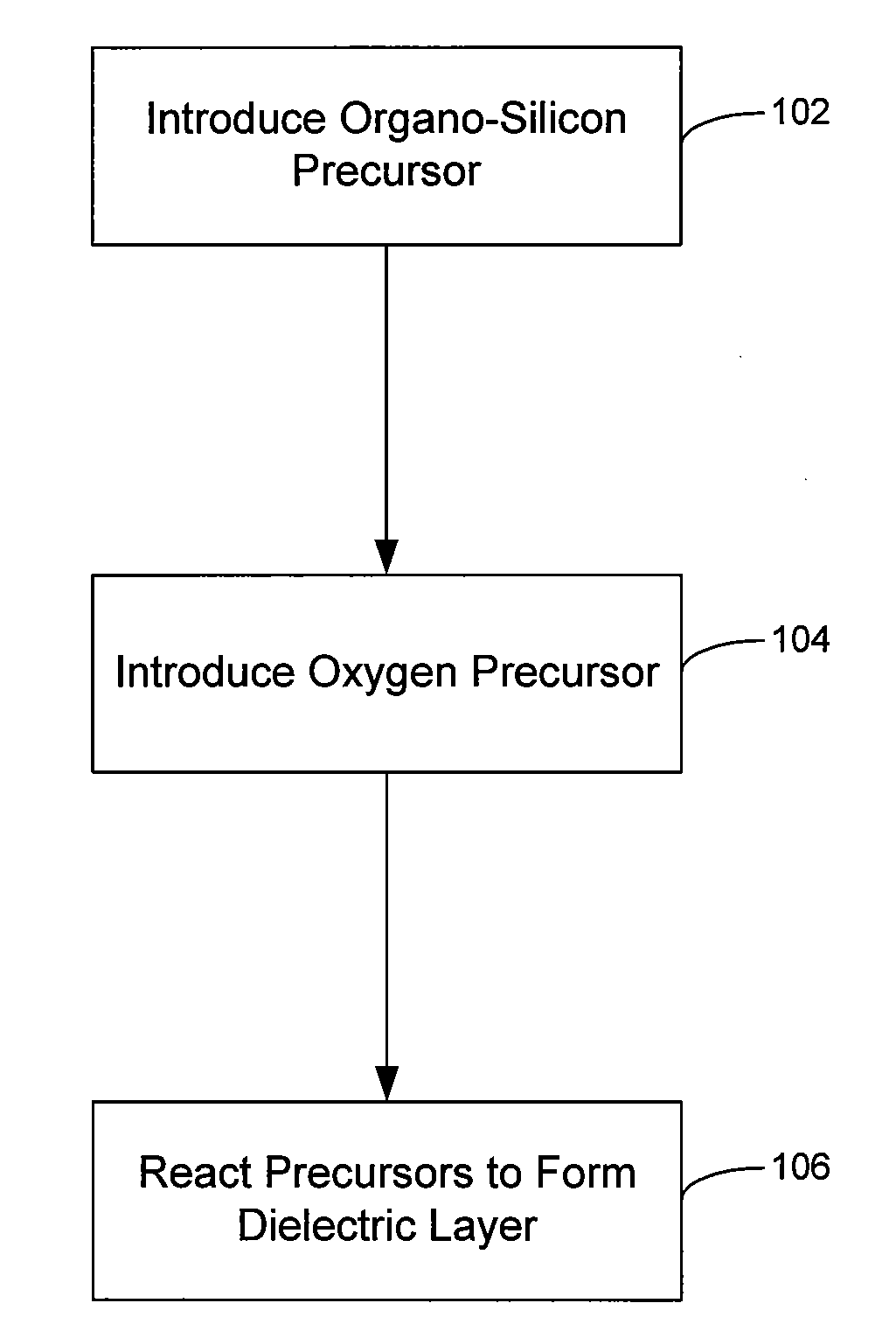
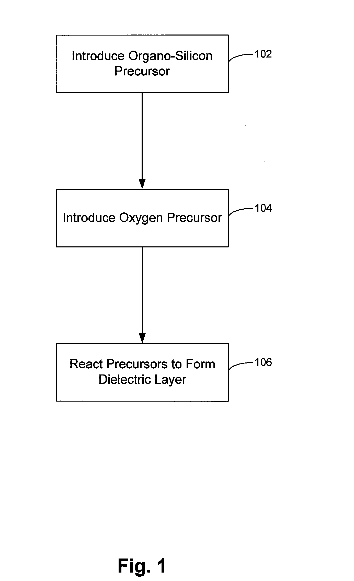
[0018]Systems and methods are described for depositing dielectric materials in gaps and on surfaces on a substrate. The dielectric materials may be formed from organo-silicon compounds that have a lower ratio of carbon atoms to silicon atoms (the C:Si ratio) than conventional tetraethoxysiloxane (TEOS). The dielectric films formed by combining these compounds with oxygen precursors typically have lower carbon contents, lower porosities, and lower WERRs than an initially deposited TEOS based silicon oxide. This makes the films less susceptible to cracking, void formation, water absorption, and / or shrinkage than TEOS based oxide films.

[0019]The organo-silicon compounds may also have a oxygen atom to silicon atom ratio (the O:Si ratio) that is equal to or greater than the TEOS O:Si ratio. Organo-silicon precursors with low C:Si ratios and high O:Si ratios produce higher quality silicon oxide films with lower carbon content than conventionally made oxides that exclusively use TEOS as a ...


PUM

PropertyMeasurementUnit
Temperatureaaaaaaaaaa
Dielectric polarization enthalpyaaaaaaaaaa

Abstract

Methods of depositing a dielectric layer in a gap formed on a substrate are described. The methods include introducing an organo-silicon precursor and an oxygen precursor to a deposition chamber. The organo-silicon precursor has a C:Si atom ratio of less than 8, and the oxygen precursor comprises atomic oxygen that is generated outside the deposition chamber. The precursors are reacted to form the dielectric layer in the gap. Methods of filling gaps with dielectric materials are also described. These methods include providing an organo-silicon precursor having a C:Si atom ratio of less than 8 and an oxygen precursor, and generating a plasma from the precursors to deposit a first portion of the dielectric material in the gap. The dielectric material may be etched, and a second portion of dielectric material may be formed in the gap. The first and second portions of the dielectric material may be annealed.

Description

CROSS-REFERENCES TO RELATED APPLICATIONS[0001]This application is related to co-assigned U.S. Provisional Patent App. Ser. No. 60 / 803,493 to Ingle et al, filed May 30, 2006, and titled “CHEMICAL VAPOR DEPOSITION OF HIGH QUALITY FLOW-LIKE SILICON DIOXIDE USING A SILICON CONTAINING PRECURSOR AND ATOMIC OXYGEN.” The application is also related to co-assigned U.S. Prov. Pat. App. Ser. No. 60 / 803,481 to Chen et al, filed May 30, 2006, and titled “A NOVEL DEPOSITION-PLASMA CURE CYCLE PROCESS TO ENHANCE FILM QUALITY OF SILICON DIOXIDE.” The application is further related to co-assigned U.S. Prov. Pat. App. Ser. No. 60 / 803,489 to Munro et al, filed May 30, 2006, and titled “A METHOD FOR DEPOSITING AND CURING LOW-K FILMS FOR GAPFILL AND CONFORMAL FILM APPLICATIONS.” The application is still further related to co-assigned U.S. Prov. Pat. App. Ser. No. 60 / 805,573 to Lubomirsky, filed Jun. 22, 2006, and titled “DIELECTRIC DEPOSITION AND ETCH BACK PROCESSES FOR BOTTOM UP GAP FILL.” The entire co...

Claims


Application Information

Patent Timeline
IPC IPC(8): H01L21/31
CPCC23C16/045Y10S438/931C23C16/452C23C16/45525C23C16/45553H01L21/02164H01L21/022H01L21/02216H01L21/02274H01L21/0234H01L21/02348H01L21/3105H01L21/31116H01L21/3122H01L21/31612H01L21/31633H01L21/76224C23C16/401C23C16/18C23C16/44
Inventor MALLICK, ABHIJIT BASUMUNRO, JEFFREY C.NEMANI, SRINIVAS D.
Owner APPLIED MATERIALS INC
Why Eureka
Try Eureka