Semiconductor device and IC label, IC tag, and IC card having the same

a technology of semiconductor devices and ic tags, which is applied in the direction of electrical signalling details, mechanical actuation of burglar alarms, instruments, etc., can solve the problems of inability to generate the power necessary for transmitting and receiving individual information, and difficulty in transmitting and receiving signals. , to achieve the effect of preventing deterioration over time of batteries, shortening the communication distance with readers/writers, and reducing the power consumption of batteries

Active Publication Date: 2007-12-13
SEMICON ENERGY LAB CO LTD
View PDF35 Cites 146 Cited by
  • Summary
  • Abstract
  • Description
  • Claims
  • Application Information

AI Technical Summary

Benefits of technology

[0027]A semiconductor device of the present invention has a power supply circuit provided with a battery; therefore, the battery can be charged periodically and shortage of power for transmitting and receiving individual information in accordance with deterioration over time of a battery can be prevented. In addition, in charging the battery, the semiconductor device of the present invention receives power in an antenna circuit provided in an RFID so that the battery is charged. Therefore, the semiconductor device can charge the battery with the utilization of power of radio waves or electromagnetic waves from the outside as a power source for driving the RFID without being directly connected to a charger. Consequently, it becomes possible to continuously use the semiconductor device without check of remaining capacity of a battery or replacement of the battery, which is necessary in the case of an active RFID. Additionally, power for driving the RFID is always retained in the battery, whereby power which is enough for an operation of the RFID can be obtained and communication distance with the reader / writer can be extended.
[0028]In the semiconductor device of the present invention, in addition to the advantage of providing the above battery, a switching circuit is provided in the power supply circuit that supplies power to a signal control circuit which transmits and receives individual information to and from the outside to periodically control supply of power to the signal control circuit. An RFID operation can be performed intermittently by control of the supply of power to the signal control circuit in the switching circuit provided in the power supply circuit. Therefore, reduction in the power consumption of the battery can be achieved and further longtime operation can be performed even without supply of power by a wireless signal.

Problems solved by technology

However, as shown in FIG. 31, in the case of a semiconductor device having an active-type RFID provided with a battery for driving, there has been a problem in that the battery consumes over time, and eventually power necessary for transmitting and receiving individual information cannot be generated in accordance with transmission and reception of individual information and set intensity of radio waves necessary for transmission and reception of the individual information.
Accordingly, there has been a problem in that confirmation of remaining capacity of a battery and replacement of a battery are required in order to continuously use a semiconductor device having an active-type RFID provided with a battery for driving.
In addition, as shown in FIG. 32, in the case of a semiconductor device having a passive-type RFID which uses power of radio waves or electromagnetic waves (carrier waves) from the outside as a power source for driving itself, there has been a problem in that it has been difficult to transmit and receive signals a long distance and to secure power for transmitting radio waves necessary for transmission and reception of signals, so that it has been difficult to realize transmission and reception in excellent condition.
Accordingly, in order to use a semiconductor device having a passive-type RFID which uses power of radio waves or electromagnetic waves (carrier waves) from the outside as a power source, there has been a problem in that a distance between the RFID and an antenna of a reader / writer which is a power supply means has been limited to be short.

Method used


Image

  • Semiconductor device and IC label, IC tag, and IC card having the same
  • Semiconductor device and IC label, IC tag, and IC card having the same
  • Semiconductor device and IC label, IC tag, and IC card having the same

Examples


embodiment mode 1

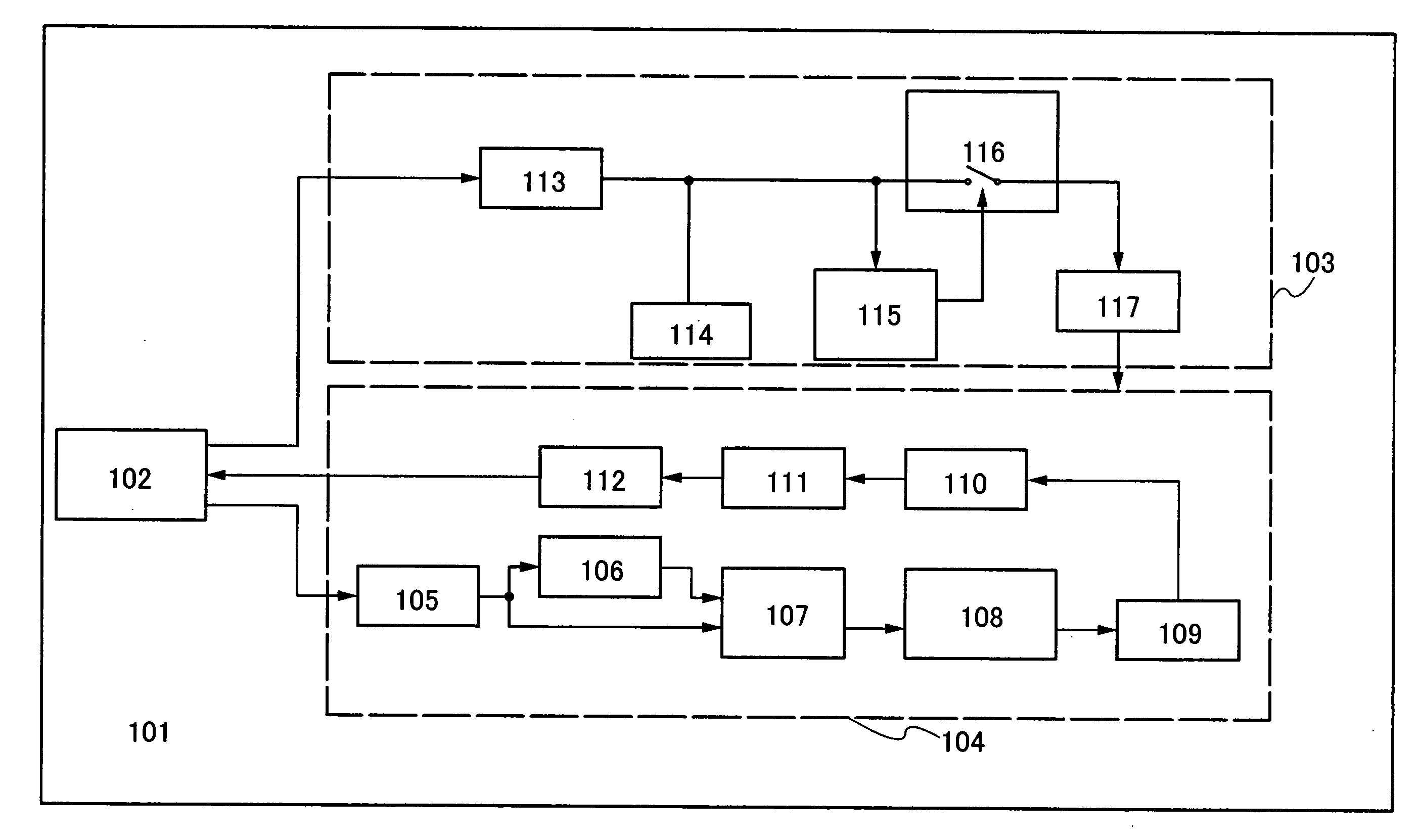
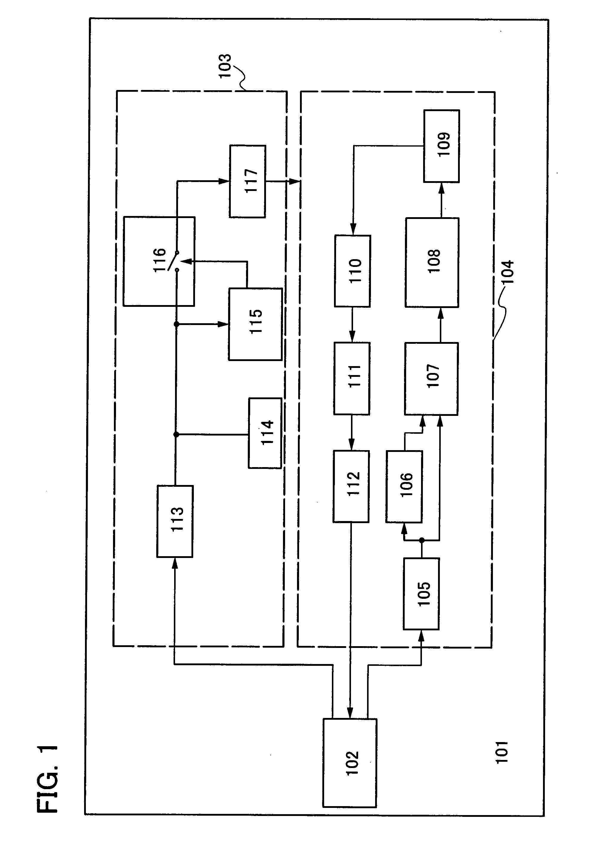
[0065]A structural example of a semiconductor device of the present invention will be explained with reference to block diagrams shown in FIGS. 1 and 2. Note that, in this embodiment mode, explanation is made of a case where a semiconductor device is used as an RFID tag (hereinafter, also simply referred to as an “RFID”).

[0066]A semiconductor device shown in FIG. 1 (hereinafter, described as an “RFID 101”) includes an antenna circuit 102, a power supply circuit 103, and a signal control circuit 104. The signal control circuit 104 includes an amplifier circuit 105, a demodulation circuit 106, a logic circuit 107, a memory control circuit 108, a memory circuit 109, a logic circuit 110, an amplifier circuit 111, and a modulation circuit 112. In addition, the power supply circuit 103 includes a rectifier circuit 113, a battery 114, a low-frequency signal generation circuit 115, a switching circuit 116, and a power source circuit 117.

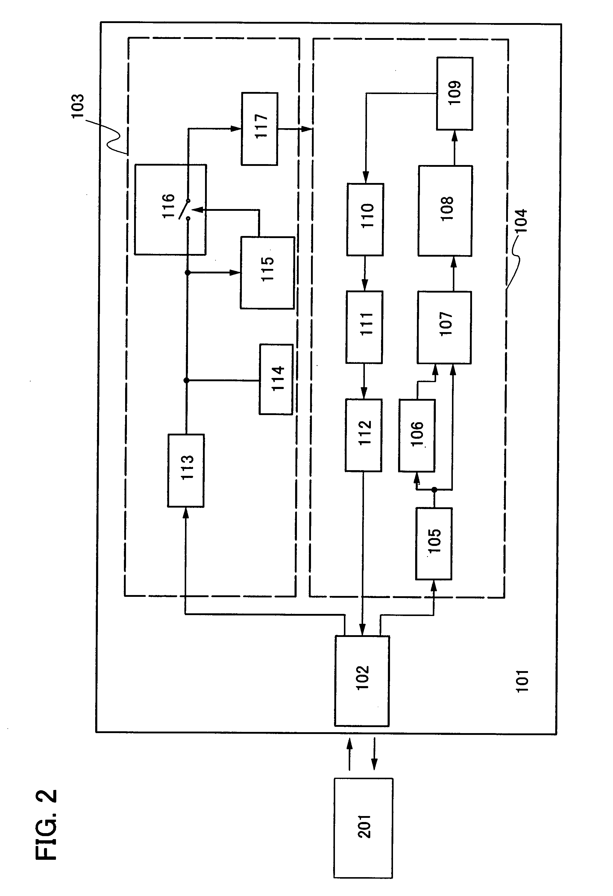
[0067]FIG. 2 shows a block diagram where the antenna c...

embodiment mode 2

[0100]This embodiment mode will explain a semiconductor device, which is the RFID having the structure described in Embodiment Mode 1 of the above, and additionally having a control circuit for controlling selection between power supplied from the rectifier circuit and that supplied from the battery, as power supplied to the power source circuit of the power supply circuit, with reference to drawings. Note that, as for the drawings used in this embodiment mode, the same portions as those in Embodiment Mode 1 are denoted by the same reference numerals in some cases.

[0101]One structural example of the semiconductor device of the present invention in this embodiment mode will be explained with reference to block diagrams shown in FIGS. 10 and 11. Note that this embodiment mode will explain the case where a semiconductor device is used as an RFID.

[0102]An RFID 101 of FIG. 10 includes an antenna circuit 102, a power supply circuit 103, and a signal control circuit 104. The signal control...

embodiment mode 3

[0130]This embodiment mode will explain a structure having a booster antenna circuit (hereinafter, referred to as a booster antenna) in the semiconductor device having the RFID shown in Embodiment Mode 1, with reference to drawings. Note that, in the drawings which are used in this embodiment mode, the same reference numerals denote the same portions as in Embodiment Mode 1.

[0131]Note that a booster antenna described in this embodiment mode refers to an antenna circuit (hereinafter, referred to as a booster antenna) which is larger than an antenna circuit which receives a signal from a reader / writer or a wireless signal from a charger or the like. An antenna circuit and the booster antenna resonate at a frequency band to be used and are magnetic-field coupled so that a signal generated by the reader / writer or the charger can be efficiently transmitted to a targeted RFID. Since the booster antenna is connected to a coil antenna through a magnetic field, the booster antenna is not nec...


PUM


Abstract

The present invention provides a power supply circuit provided with a battery as a power source for supplying power to an RFID, and the battery of the power supply circuit is charged with a wireless signal. Then, a switching circuit is provided in the power supply circuit that supplies power to a signal control circuit which transmits and receives individual information to and from the outside to intermittently control supply of power to the signal control circuit by a signal from a low-frequency signal generation circuit.

Description

TECHNICAL FIELD[0001]The present invention relates to a semiconductor device. In particular, the present invention relates to a semiconductor device which transmits and receives data through radio waves and receives power. Further, the present invention relates to a communication system through radio waves and using a semiconductor device, an antenna and a reader / writer which transmit and receive data to and from the semiconductor device, and an antenna and a charger which supply power to the semiconductor device.[0002]Note that semiconductor devices in this specification refers to all devices which can function with the use of a semiconductor characteristic.BACKGROUND ART[0003]In recent years, an individual identification technique using wireless communication using an electromagnetic field, a radio wave, or the like has attracted attention. In particular, an individual identification technique with the utilization of an RFID (Radio Frequency IDentification) tag as a semiconductor ...

Claims


Application Information

Patent Timeline
Patent Type & Authority Applications(United States)
IPC IPC(8): G08B13/14H04Q5/22
CPCG06F1/263G06K19/0702G06K19/0723H04B5/0037H01L21/84H01L27/12H02J7/025G06K19/07749G06F1/26G06K19/07H01L27/06H02J50/10H02J50/80
Inventor KOYAMA, JUN
Owner SEMICON ENERGY LAB CO LTD
Why Eureka
Try Eureka