Semiconductor device

a technology of semiconductor devices and semiconductors, applied in the direction of generators/motors, mechanical actuation of burglar alarms, instruments, etc., can solve the problems of power shortage, inability to check the remaining capacity of the cell, and the inability to generate electronic power for individual information transmission and reception, etc., to achieve the effect of increasing the communication range with the reader/writer and power shortag

Inactive Publication Date: 2014-04-08
SEMICON ENERGY LAB CO LTD
View PDF89 Cites 10 Cited by
  • Summary
  • Abstract
  • Description
  • Claims
  • Application Information

AI Technical Summary

Benefits of technology

[0018]A semiconductor device of the invention includes the battery and the power generation element. Therefore, power shortage in accordance with deterioration of the battery over time, which occurs in a conventional active type RFID, can be prevented. Further, in a semiconductor device of the invention, an electric power can be supplied to the battery from the power generation element; therefore, the semiconductor device can be used continuously without a check of remaining capacity of the battery and a change of the battery. In addition, since electric power for driving the RFID is held in the battery, electric power sufficient to drive the RFID can be obtained and a communication range with the reader / writer can be increased.

Problems solved by technology

However, as shown in FIG. 29, in a case of a semiconductor device including an active type RFID provided with a cell for driving, there has been a problem in that the cell is used up over time in accordance with transmission and reception of individual information or setting of intensity of a radio wave required for transmission and reception of individual information, and finally, an electronic power required for transmission and reception of individual information cannot be generated.
Consequently, there has been a problem in that a check of remaining capacity of the cell and a change of the cell are required in order to continuously use the semiconductor device including the active type RFID provided with the cell for driving.
In addition, as shown in FIG. 30, in a case of a semiconductor device including a passive type RFID in which electric power for driving is made by using an external radio wave or electromagnetic wave (carrier wave), there has been a problem in that it is difficult to secure electric power required for transmission and reception of a long-distance signal and for transmitting an electric wave required for transmission and reception; therefore, it is difficult to obtain a favorable transmission / reception state.
Consequently, there has been a problem in that the semiconductor device including the passive type RFID in which the power supply for driving is made by using electric power from an external radio wave or electromagnetic wave (carrier wave) can be used only within a short distance from an antenna of a reader / writer, which is a power supply unit capable of supplying enough an electric power from an external radio wave or electromagnetic wave (carrier wave).

Method used


Image

  • Semiconductor device
  • Semiconductor device
  • Semiconductor device

Examples


embodiment mode 1

[Embodiment Mode 1]

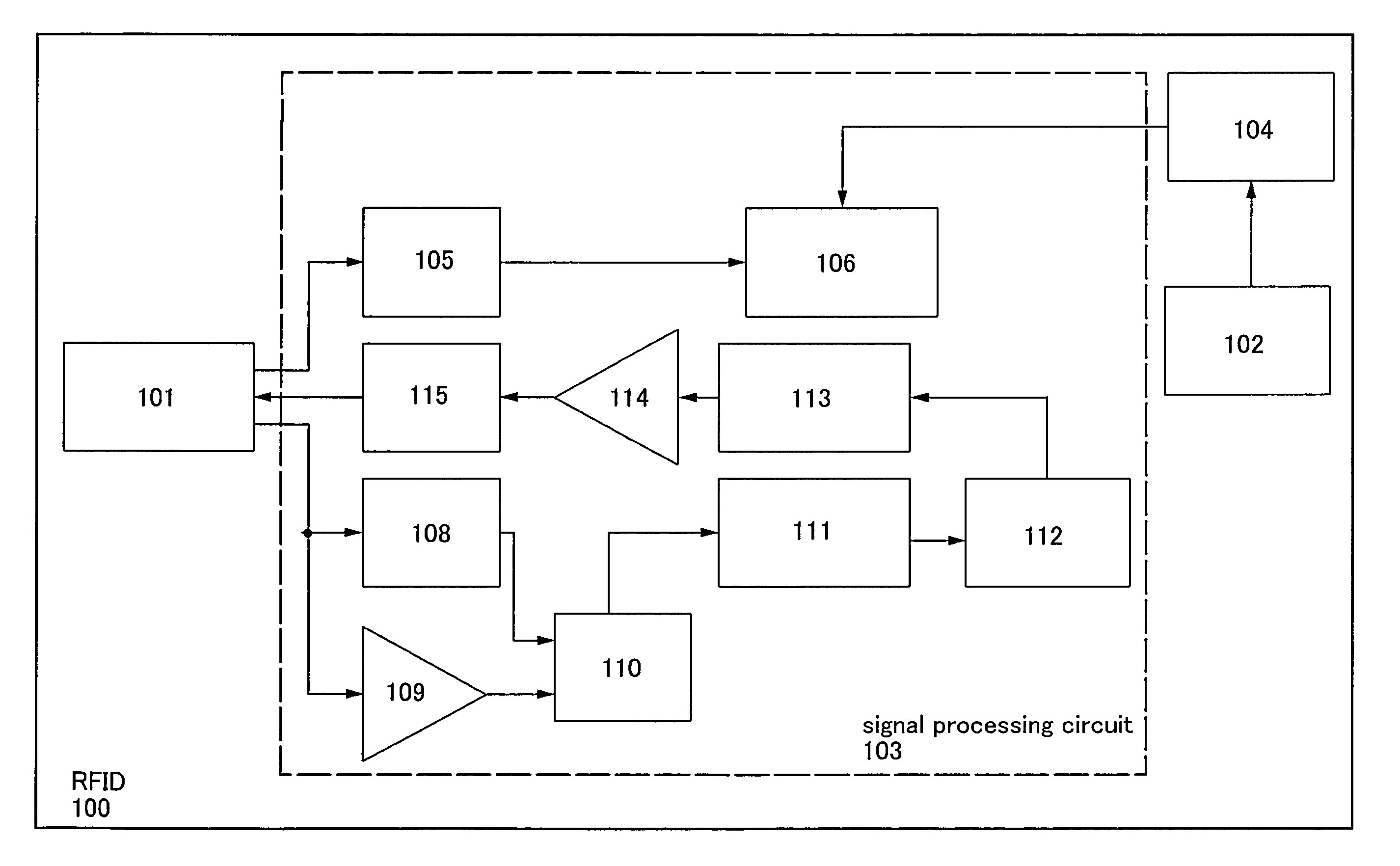
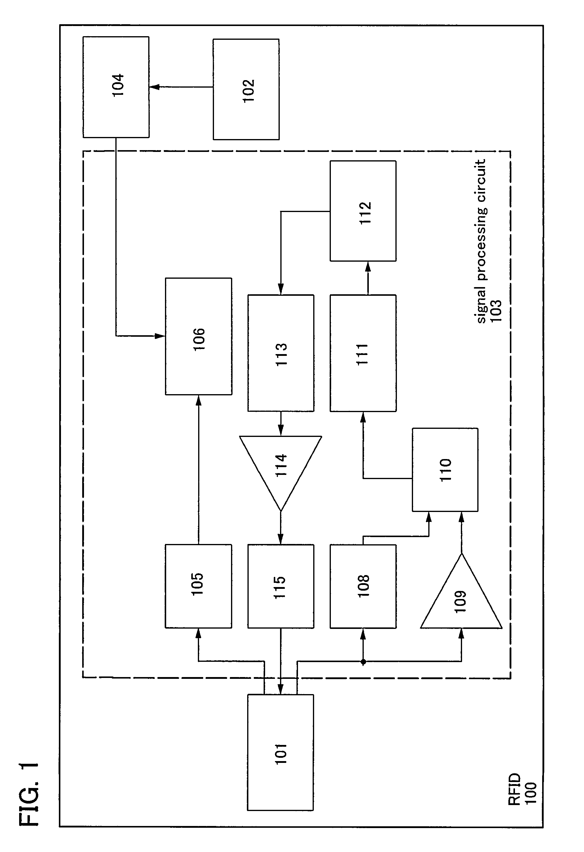
[0050]A semiconductor device used for an RFID of the invention is described using block diagrams shown in FIGS. 1 and 2.

[0051]An RFID 100 in FIG. 1 includes an antenna circuit 101, a power generation element 102, a signal processing circuit 103, and a battery 104. The signal processing circuit 103 includes a rectifier circuit 105, a power supply circuit 106, a demodulation circuit 108, an amplifier 109, a logic circuit 110, a memory control circuit 111, a memory circuit 112, a logic circuit 113, an amplifier 114, and a modulation circuit 115. Electric power obtained by the power generation element 102 is input to the battery 104, and is supplied to the power supply circuit 106 from the battery 104 as appropriate.

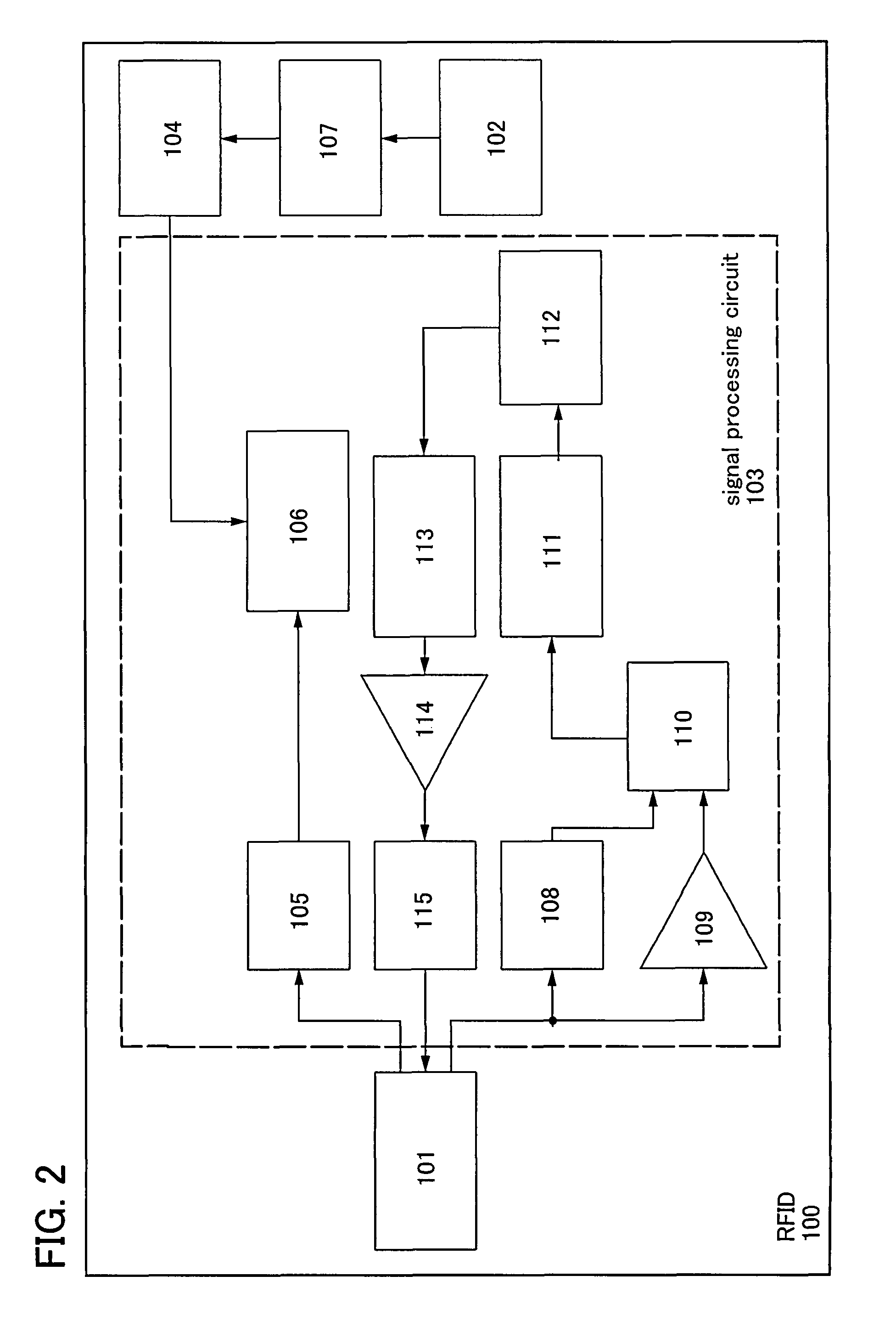
[0052]When the electric power obtained by the power generation element 102 is an alternating-current voltage, as shown in FIG. 2, the obtained alternating-current voltage is converted to a direct-current voltage through a rectifier circuit 107, and subsequ...

embodiment mode 2

[Embodiment Mode 2]

[0091]In this embodiment mode, in the semiconductor device including the RFID shown in Embodiment Mode 1, a structure where a booster antenna circuit (hereinafter referred to as a booster antenna) is included is described with reference to drawings. Note that the same portions as Embodiment Mode 1 are denoted by the same reference numerals and description of such portions is omitted.

[0092]Note that a booster antenna described in this embodiment mode is a larger antenna (hereinafter referred to as a booster antenna) than an antenna (hereinafter referred to as a chip antenna or an antenna circuit) which receives a signal from a reader / writer included in the semiconductor device and outputs the signal to a signal processing circuit of the RFID. The booster antenna is an antenna which can efficiently transmit a signal oscillated by a reader / writer or a battery charger to an objective RFID by being resonated in a frequency band in which the booster antenna is used, and...

embodiment mode 3

[Embodiment Mode 3]

[0106]In this embodiment mode, an example of a manufacturing method of the semiconductor device shown in the aforementioned embodiment modes is described with reference to drawings. In this embodiment mode, a case where the thermoelectric element shown in FIG. 7B is used as a power generation element is described by using a cross sectional view along a line A-B of the thermoelectric element in FIG. 7B.

[0107]First, as shown in FIG. 17A, a peeling layer 1903 is formed on one surface of a substrate 1901 with an insulating film 1902 interposed therebetween, and sequentially, an insulating film 1904 functioning as a base film and a semiconductor film 1905 (for example, a film containing amorphous silicon) are stacked thereover. Note that the insulating film 1902, the peeling layer 1903, the insulating film 1904, and the semiconductor film 1905 can be continuously formed.

[0108]The substrate 1901 is selected from a glass substrate, a quartz substrate, a metal substrate (...


PUM


Abstract

Objects of the invention are to provide a semiconductor device including an RFID, which can transmit and receive individual information without a check of remaining capacity of the battery and a change of the battery in accordance with deterioration over time of the battery for a driving power supply; and which maintains a favorable communication state even when electric power, as a power supply for driving, from an external radio wave or electromagnetic wave (carrier wave) is not sufficient. A battery is provided as a power supply for supplying electric power in the RFID, and electric power obtained by a power generation element is charged in the battery.

Description

TECHNICAL FIELD[0001]The present invention relates to a semiconductor device. In particular, the present invention relates to a semiconductor device which transmits and receives data through a radio wave and includes a small power generation element. Further, the present invention relates to a communication system using the semiconductor device, and an antenna and a reader / writer which transmit and receive data to and from the semiconductor device.[0002]Note that in this specification, a semiconductor device indicates any device which can function by using semiconductor characteristics.BACKGROUND ART[0003]Nowadays, an individual identification technology using wireless communication through an electromagnetic field, a radio wave, or the like has attracted attention. In particular, as a semiconductor device which communicates data by wireless communication, an individual identification technology using an RFID (Radio Frequency Identification) tag has attracted attention. An RFID tag ...

Claims


Application Information

Patent Timeline
Patent Type & Authority Patents(United States)
IPC IPC(8): H04Q5/22
CPCG06K19/0707G06K7/10178G06K19/0705H01Q1/38H01Q9/285H01Q1/2225H01Q7/00H01Q1/36G06K19/0723H02N2/186
Inventor SHIONOIRI, YUTAKAIZUMI, KONAMIKOYAMA, JUNKUROKAWA, YOSHIYUKIYAMAZAKI, SHUNPEIATSUMI, TOMOAKIOSADA, TAKESHIIKEDA, TAKAYUKIISHII, MASATO
Owner SEMICON ENERGY LAB CO LTD
Why Eureka
Try Eureka