

Method of measuring minority carrier diffusion length and method of manufacturing silicon wafer
a minority carrier and diffusion length technology, applied in the direction of individual semiconductor device testing, semiconductor/solid-state device testing/measurement, instruments, etc., can solve the problems of inability to obtain accurate measurements, the surface of the wafer is not stable immediately, and the device characteristics of the finished product are negatively affected, etc., to achieve rapid and reliable measurement of minority carrier diffusion length
- Summary
- Abstract
- Description
- Claims
- Application Information
AI Technical Summary
Benefits of technology
Problems solved by technology
Method used
Image

Examples
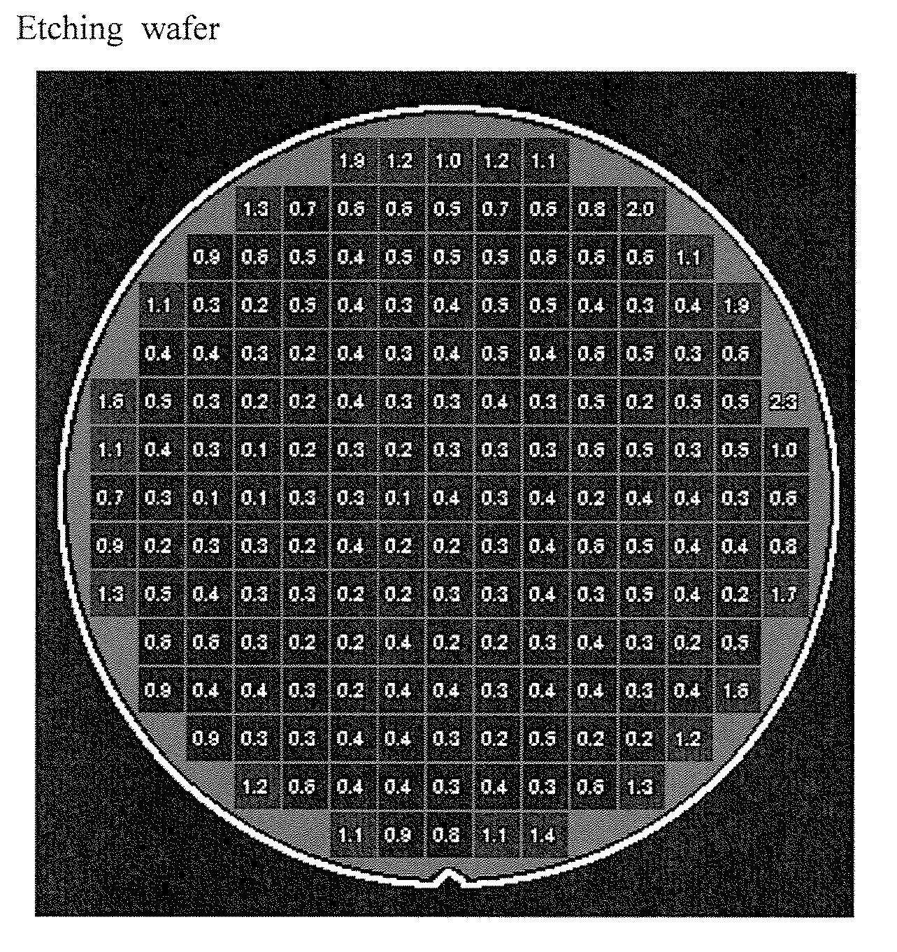
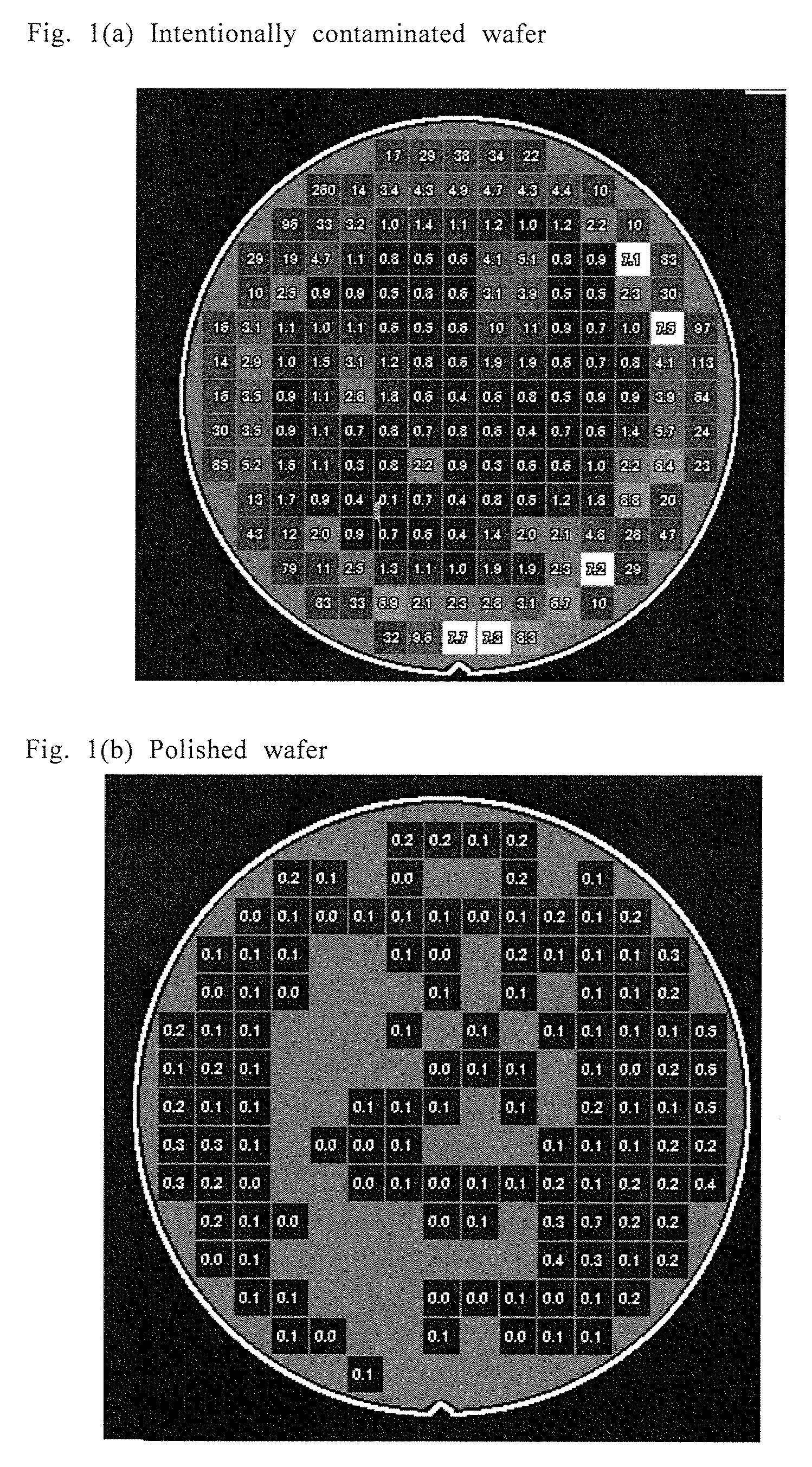
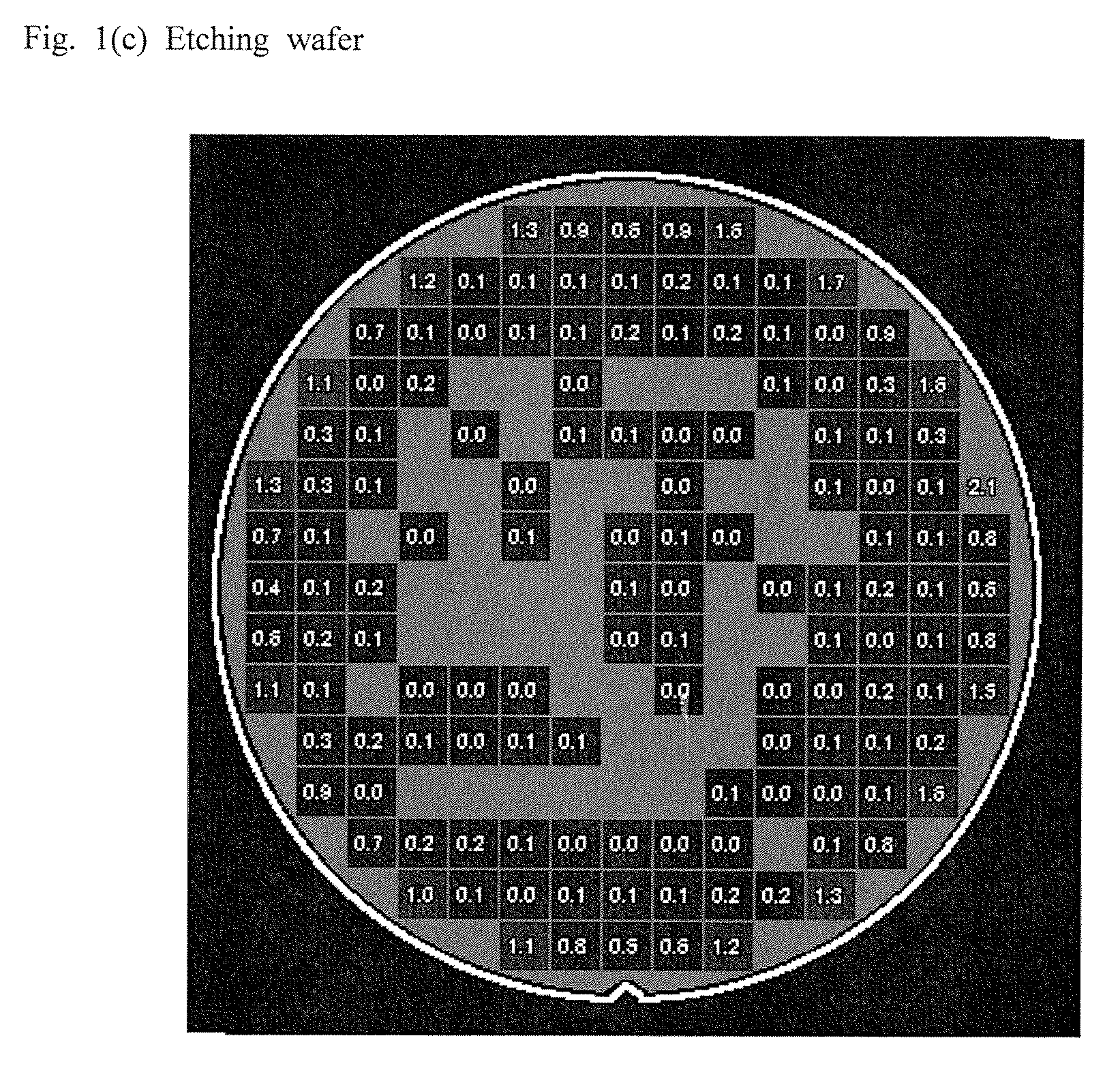
example 1
[0056] Each of the wafers that had been subjected to the SPV measurement in Comparative Example 1 was left standing for one week, retreated with HF, and immersed for 5 seconds in a vat filled with a diluted solution of p-tert-octylphenoxy polyethyl (a carbon-containing compound). The wafers were then dried with an N2 purge. The diluted solution was obtained by diluting the original solution 1,000-fold with water. The original solution was a mixed solution comprising 25 to 30 weight percent of p-tert-octylphenoxy polyethyl, 30 to 40 weight percent of water, and 37 weight percent of ethylene glycol. Following the above-described treatment, the surfaces of the wafers were irradiated for 45 seconds with ultraviolet radiation (wavelength 185-254 nm, approximate intensity 8 mW) in an oxygen-containing atmosphere (air), and immediately subjected to SPV measurement. The energy of the ultraviolet radiation was 647 kJ / mol at a wavelength of 185 nm and 472 kJ / mol at a wavelength of 254 nm. Ban...
PUM
 Abstract
Description
Claims
Application Information