Variable resistance random access memory device and a method of fabricating the same

a random access memory and variable resistance technology, applied in semiconductor devices, digital storage, instruments, etc., can solve the problems of reducing affecting the stability affecting the reliability of non-volatile variable resistance memory devices, etc., to achieve stable reset current, lower manufacturing cost, and high integration memory

Active Publication Date: 2007-12-27
SAMSUNG ELECTRONICS CO LTD
View PDF1 Cites 166 Cited by
  • Summary
  • Abstract
  • Description
  • Claims
  • Application Information

AI Technical Summary

Benefits of technology

[0012]Example embodiments provide a non-volatile memory device, for example, variable resistance random access memory device, that may have a relatively stable reset current even though switching operations may be repeated by including a buffer layer between a lower electrode and a variable resistance oxide layer and an n+ interfac

Problems solved by technology

However, stored data may be erased after power is turned off.
As the switching cycles are repeated, the resistance state of the oxide layer 14 may continuously change and an operating voltage and a reset voltage may increase, thereby

Method used


Image

  • Variable resistance random access memory device and a method of fabricating the same
  • Variable resistance random access memory device and a method of fabricating the same
  • Variable resistance random access memory device and a method of fabricating the same

Examples


Embodiment Construction

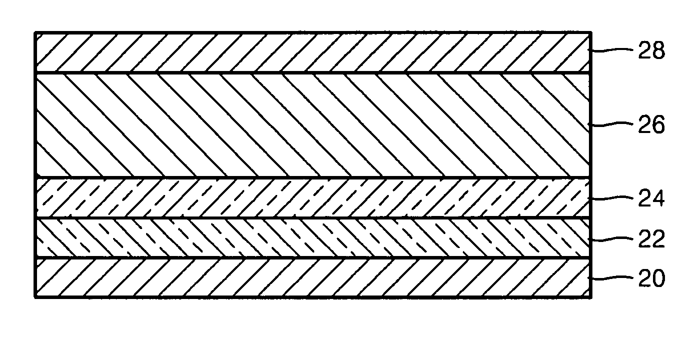
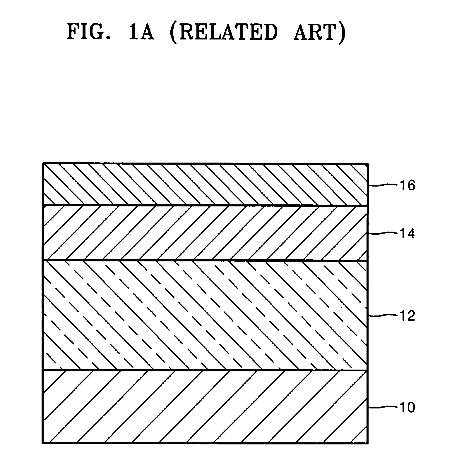
[0026]Hereinafter, a variable resistance random access memory device having an n+ interfacial layer according to example embodiments will now be described with reference to accompanying drawings. In the drawings, the thicknesses and widths of layers and regions are exaggerated for clarity.

[0027]It will be understood that when an element or layer is referred to as being “on,”“connected to” or “coupled to” another element or layer, it can be directly on, connected or coupled to the other element or layer or intervening elements or layers may be present. In contrast, when an element is referred to as being “directly on,”“directly connected to” or “directly coupled to” another element or layer, there are no intervening elements or layers present. Like reference numerals refer to like elements throughout. As used herein, the term “and / or” includes any and all combinations of one or more of the associated listed items.

[0028]It will be understood that, although the terms first, second, thi...


PUM


Abstract

Provided is a variable resistance random access memory device having an n+ interfacial layer and a method of fabricating the same. The variable resistance random access memory device may include a lower electrode, an n+ interfacial layer on the lower electrode, a buffer layer on the n+ interfacial layer, an oxide layer on the buffer layer and having a variable resistance characteristic and an upper electrode on the oxide layer.

Description

PRIORITY STATEMENT[0001]This application claims priority under 35 USC § 119 to Korean Patent Application No. 10-2006-0058098, filed on Jun. 27, 2006, in the Korean Intellectual Property Office (KIPO), the entire contents of which are incorporated herein by reference.BACKGROUND[0002]1. Field[0003]Example embodiments relate to a non-volatile memory device and a method of fabricating the same. Other example embodiments relate to a variable resistance random access memory device that is operated at a lower operating voltage by including an n+ interfacial layer between a lower electrode formed of a common metal and a buffer layer and a method of fabricating the same.[0004]2. Description of the Related Art[0005]Semiconductor memory devices may have higher integration density, faster operation speeds and lower operating voltage. A conventional memory device may include a plurality of circuitry connected to memory cells. In the case of dynamic random access memory (DRAM), which is represent...

Claims


Application Information

Patent Timeline
IPC IPC(8): H01L47/00H01L21/00
CPCH01L45/12Y10S438/90H01L45/146H01L45/1233H01L45/04H10N70/801H10N70/20H10N70/826H10N70/8833G11C13/0004
Inventor CHO, CHOONG-RAELEE, EUN-HONGGENRIKH, STEFANOVICHBOURIM, EL MOSTAFA
Owner SAMSUNG ELECTRONICS CO LTD
Why Eureka
Try Eureka