

Display device
- Summary
- Abstract
- Description
- Claims
- Application Information
AI Technical Summary
Benefits of technology
Problems solved by technology
Method used
Image

Examples
first embodiment
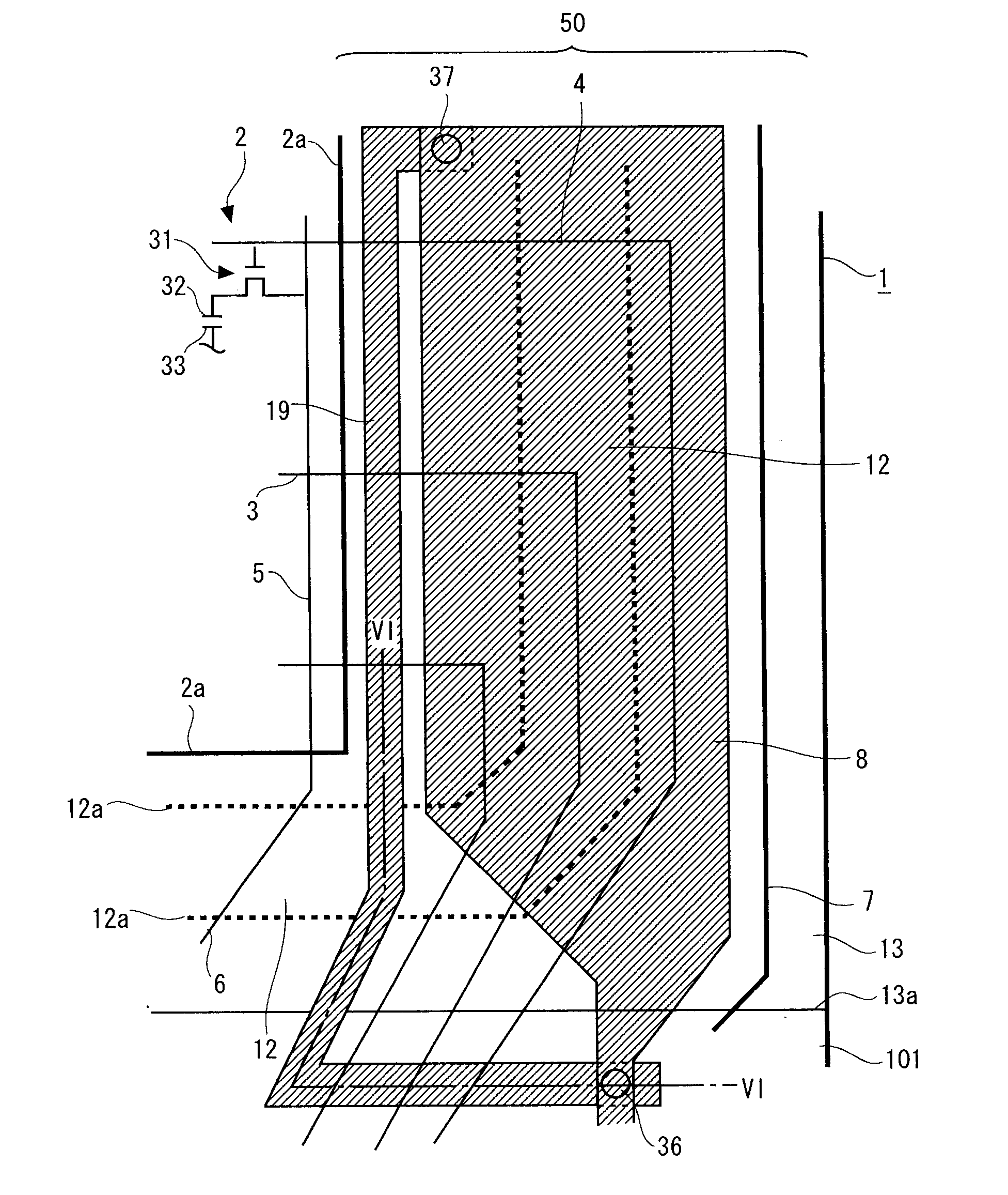
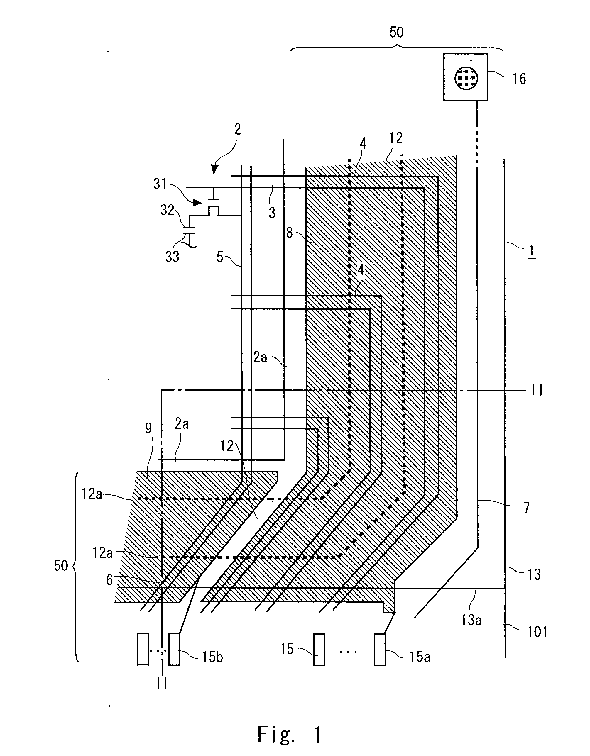
[0032] A liquid crystal display device according to a first embodiment of the present invention includes liquid crystal filled in between a TFT array substrate and an opposing substrate. Then, the TFT array substrate and the opposing substrate are bonded to each other with a sealing material applied around a display region like a frame. The TFT array substrate has scanning signal lines and display signal lines. A first conductive layer is formed over the scanning lead-out lines connected to the scanning signal lines. The first conductive layer is formed to cover the scanning lead-out lines outside at least the sealing material and applied with a predetermined potential. Incidentally, in this embodiment, an active matrix type liquid crystal display device is described below as an example of the display device, but the present invention is not limited to the active matrix type liquid crystal display device. That is, the present invention is applicable to any display device having a di...
second embodiment
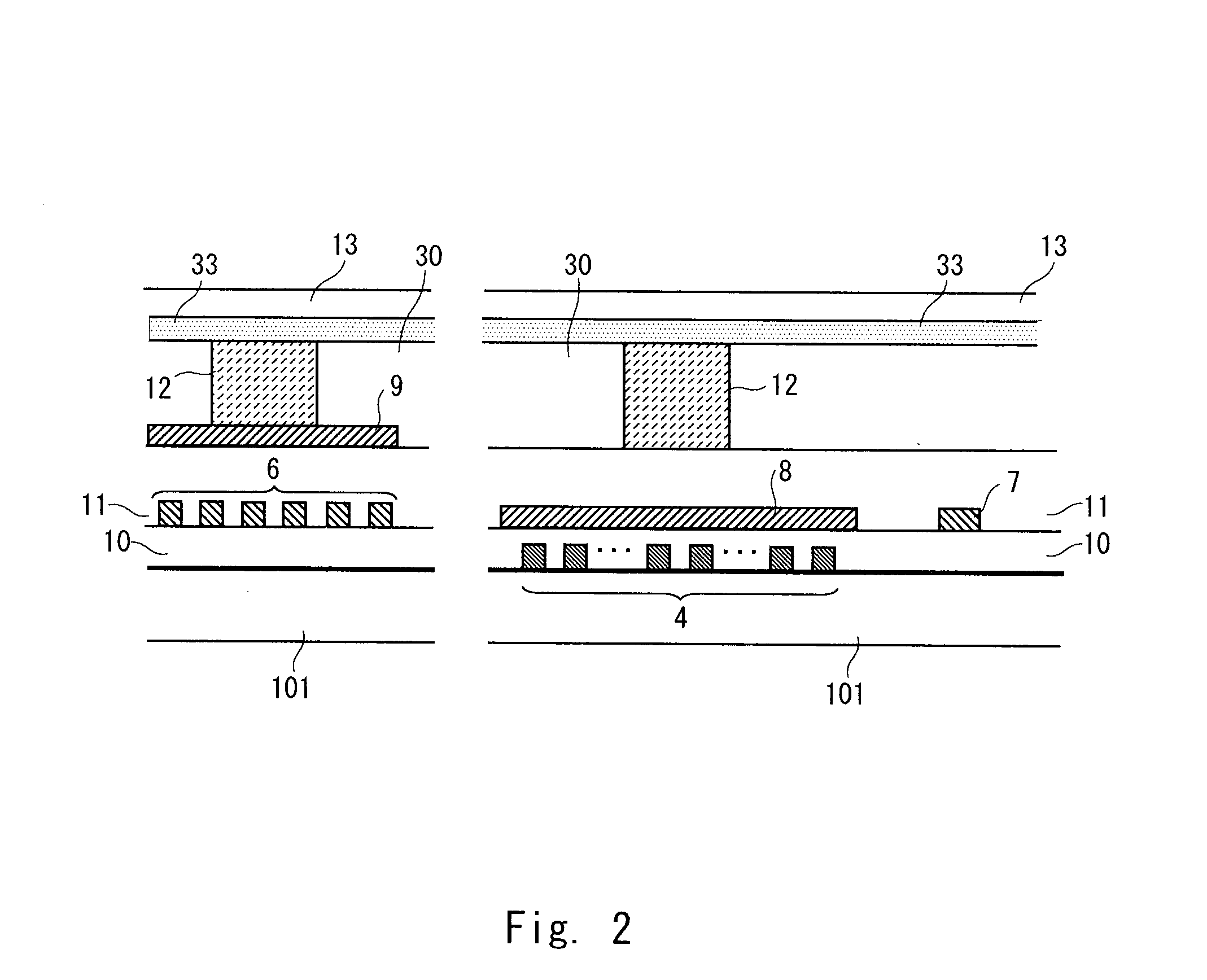
[0060] In this embodiment, a liquid crystal display device is described as an example of the display device similar to the first embodiment. Referring to FIGS. 5 and 6, the liquid crystal display device of this embodiment is described. FIG. 5 is a plan view of the structure of an end portion of the liquid crystal panel 1, and FIG. 6 is a sectional view taken along the line VI-VI of FIG. 5. Incidentally, the basic structure of the liquid crystal display device of this embodiment is the same as the first embodiment, so its description thereof is omitted. For example, first conductive layer 8 is formed to cover almost all of the scanning lead-out line 4 outside the sealing material 12.
[0061] Further, the liquid crystal TFT array substrate 101 of the display device of this embodiment has a repair pattern 19 as shown in FIG. 5. The repair pattern 19 can repair the short-circuited portion of the scanning lead-out line 4. The repair pattern 19 is formed closer to the display region 2 side...
third embodiment
[0070] In this embodiment, a liquid crystal display device is described as an example of the display device similar to the first embodiment. Referring to FIGS. 8 and 9, the liquid crystal display device of this embodiment is described. FIG. 8 is a plan view of the structure of an end portion of the liquid crystal panel 1, and FIG. 9 is a sectional view taken along the line IX-IX of FIG. 8. Incidentally, the basic structure of the liquid crystal display device of this embodiment is the same as the first embodiment, so its description thereof is omitted. That is, first conductive layer 8 is formed to cover almost all of the scanning lead-out line 4 outside the sealing material 12.
[0071] In this embodiment, the scanning lead-out line 4 is covered with a third conductive layer 28 as well as the first conductive layer 8. Here, the third conductive layer 28 covers the scanning lead-out line 4 just below the pattern of the sealing material 12. Accordingly, the first conductive layers 8 ar...
PUM
 Abstract
Description
Claims
Application Information